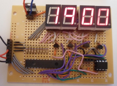
MCP23017 8-segment LED timer
28 December 2017This circuit is a second attempt at creating a 8-segment LED version of my LCD-based timer circuit, as the previous attempt had too many issues for it to be completed. This time round I am using a single 16-bit I/O expander (Microchip
MCP23017) rather than two 8-bit I/O expanders (TI PCF8574), so much of the article will discuss usage of this part I had stocked but until now not used in a circuit. The other design decisions, such use of LS0565SRWK LED chips (Farnell 2627645) and MC01010 prototyping board (Farnell 2768280), are the same as those taken previously.
Circuit layout
Much like the previous attempt all the corresponding segments within each LED chips are connected to a common current source, and each chip's ground is connected to a current sink — this in turn reflects the row-driver & column driver architecture used in my LED matrix display. TheMCP23017 is a current source rather than being open-drain like the previously-used PCF8574, so it supplies the segment power directly, and low-side NPN transistors are used as current sinks — previously high-side PNP transistors supplied the current and expanders acted as grounding sinks. As can be seen below the design (right image) is not that far off that for the previous layout (left image), although it does omit some late-stage additions & changes.
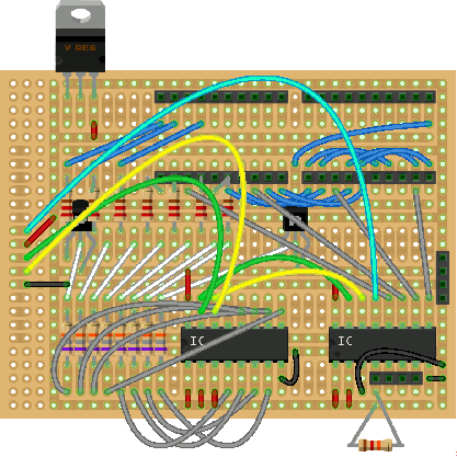
I have to admit that, at least when using these particular prototyping boards, I only use Fritzing to get rough sizing rather than doing waterfall design. I did update the design as I went along, but clearly a few late-stage changes & additions were not included. I am not sure if this circuit actually needed I2C pull-up resistors, but a quick mess-around with my LED matrix controller suggested that they might be required, so I added them in just to eliminate it as a possible complication. To my knowledge a lot of I2C driver circuitry is open-drain, so something somewhere along the line needs to hold the signal lines high — most of the time I am using a I2C -USB adapters, which most likely have these built-in.
Component ratings
TheMCP23017 I/O expanders support a maximum of 25mA through each output pin and a total chip draw of 150mA, so I assumed it would be safe for each pin to source 10mA. Rather bliuntly assuming a 5-volt potential difference I opted to use a 470Ω resisitor to limit the current draw to a nominal 10.63mA, which implies a total current of 85mA if all segments are switched on. The BC547B NPN through-hole transistor (Farnell 2453790) has a gain of 200 which according to the data-sheet graphs does not reduce significantly until the collector current gets close to the transistor's 100mA limit. Again assuming 5 volts I opted for a 12kΩ transistor base resisitor which results in nominal base current of 0.41mA, and hence a collector current of 83mA. The LED chip data-sheet recommends an operating current of 20mA which I am pretty sure is per-chip, but since the above 83mA is a continous-current value rather than the actual 25% duty cycle, the power dissipation is about the same at 35mW — below the 85mW stated limit for the LED chip.
In practice the actual per-segment continious current was 5.4mA giving a total 8-segment power draw of 42.7mA, which is about half the expected values — the cause was not accounting for the voltage drops across the other components, so the assumed voltages across the resistors were over-estimated. The approximate electrical path for each of the LED segments is shown below, along with measurments taken using a multi-meter:
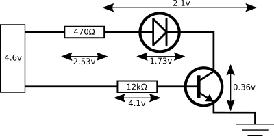
The measurements were taken independently, so overlapping voltage drops might not sum up exactly. I went digging through the data-sheets to see what extent I could have known in advance these electrical characteristics, and my conclusions are listed.
- Voltage regulator output
- The voltage regulator has a rated output of 5 volts, and was measured at 4.97 volts — I am inclined to believe a small amount of resistance in wiring accounts for this difference, which in my mind is basically negligable.
- Expander voltage output
- Within the data-sheet parameter D090 (output high-voltage) is stated as a mimimum of Vdd-0.7 (i.e. 4.3 volts in a 5 volt circuit) and no typical value is given. The voltage between an output pin and ground was measured as 4.6 volts, which implies a voltage drop 0.4 volts. For maximum-current calculations assuming negligable voltage drop was reasonable.
- LED voltage drop
- Measured at 1.73 volts, this is the lower end of the 1.7 to 2.5 volt forward current stated in the data-sheet. Using the lower bound 1.7 volts would therefore would have been reasonable for current-limiting calculations, and omitting it entirely is the single largest avoidable factor in the mis-calculation.
- Transistor base-emitter drop
- For saturation conditions this is supposed to be between 700mV and 900mV volts for collector currents below 100mA, and for the measured 42.7mA is supposed to be a touch over 800mV volts, but in practice was only 500mV. Using 700mV for calculations would have been reasonable, given that base current calculations tend to be huge overestimates anyway, as a result of gain values being mimimums.
- Transistor collector-emitter drop
- The graph in the data-sheet for base-emitter saturation voltage has more variance than that for the base-emitter drop, and for a collector current of 40mA is supposed to be about 80mV. A table entry for IB of 0.5mA and IC of 10mA states a typical saturation VCE of 90mV and maximum 250mV — this is well below the 360mV measured across the transistor, and I am not sure how I could have even got a ball-park figure from the data-sheet.
Microchip MCP23017
This time round I will be making use of theMCP23017, which although is marketed as a 16-bit I/O expander, it is in effect two 8-bit expanders on the same chip. Each 8-bit port has a bank of registers associated with it, and by default these banks are interlaced within the register address space. They can instead be grouped together by bank/port by setting IOCON.BANK=0, but this mode is one that I currently have no interest in. By default all registers have all bits cleared (i.e. are zeroed), with the exception of IODIRA & IODIRA (I/O direction control), which have all bits set.
I will cover all available functionality of this I/O expander below, alongside some remarks on what I think of the functions, but will only go into detail for functionality I actually used for this circuit. For demonstration purposes I will assume that the Robot Electronics USB-ISS USB-I2C adapter is being used as an I2C master attached to /dev/ttyACM0, and that it is being driven using my Python Tx-Rx script which takes the following commands:
./ttyTxRx.py /dev/ttyACM0 1 55 <device> <register> <bytecount> [values]
Before using any of the control commands below, the USB adapter will need to be set to I2C mode, which can be done using the following command. Since the expander supports 400kHz, the following will also set the I2C master clock rate to this frequency (use 0x60 instead of 0x70 for 100kHz):
./ttyTxRx.py /dev/ttyACM0 2 5a 02 70
Device address
The upper four bits of theMCP23017 address are fixed to 0b0100 (i.e. 0x4), as shown in Figure 3-4 on page 15 of the data-sheet and reproduced below, the remaining three address bits are set according to the three external address pins. For this circuit all three address pins are tied to ground so the lower bits of the device address are all zeros. Using the convention that the Read/Write bit is included in the address octet, this means for the circuit the device address is 0x40.
| MSB | Bit 6 | Bit 5 | Bit 4 | Bit 3 | Bit 2 | Bit 1 | LSB |
| 0 | 1 | 0 | 0 | A2 | A1 | A0 | R/W |
Setting pin direction
Pin direction (i.e. input or output) for the two ports is controlled byIODIRA & IODIRB which use the addresses 0x00 & 0x01 respectively. A set bit indicates input and a cleared bit indicates output, and unlike all the other registers these are initially all set high (i.e. all pins are input). For this circuit, all pins except the lower four of port B need to be set to output:
./ttyTxRx.py /dev/ttyACM0 1 55 40 00 1 00 ./ttyTxRx.py /dev/ttyACM0 1 55 40 01 1 0f
Enabling pull-up
One interesting feature is that there are built-in pull-up resistors that can optionally be enabled per-pin on pins that are acting as input. These are controlled byGPPUA & GPPUB which are at 0x00 & 0x01 respectively, and a weak 100kΩ pull-up is enabled when the corresponding bit is set high. For this circuit, enable it for all pins on port B (register has no effect on output pins):
./ttyTxRx.py /dev/ttyACM0 1 55 40 0d 1 0f
I was going to include external 2kΩ pull-down resistors, so finding out about the built-in pull-ups was nice because space is already quite tight on this circuit, and in any case I can disable them if I later decide to use buttons that have their own pull-up/pull-down resistors. It did mean a change from press-is-on to press-is-off for the input handling, but this is a minor point. Only concern is that 100kΩ is a bit on the weak side for my liking, as in some long-running tests I have seen tied-high pins momentaraly flip low.
Reading & writing pins
Pin values are read and written via theGPIOA & GPIOB registers which use the addresses 0x12 & 0x13 respectively. Note that any output pins will need to be masked out. Setting the upper four pins of each port can be done using the following:
./ttyTxRx.py /dev/ttyACM0 1 55 40 12 1 f0 ./ttyTxRx.py /dev/ttyACM0 1 55 40 13 1 f0
and conversely, for reading port B (note use of 0x41 rather than 0x40 for the device address):
./ttyTxRx.py /dev/ttyACM0 1 55 41 13 1
There are also the OLATA & OLAT registers (0x14 & 0x15) which expose the state of the output latches, but since a write to GPIOx is an implicit write to OLATx I am not sure they have any practical use being exposed — all they really do is let you read back a previously written value.
Reading/writing multiple bytes
Even though registers are single bytes, multiple bytes can be read or written in a single I2C transaction. With the defaultIOCON.BANK=0 (bank registers are interlaced) and IOCON.SEQOP=0 (sequential operation disabled), the second read/write will access the same register within the other bank, and access will toggle between the two. As an example the following will write 0x00 to GPIOB, then 0xff to 0x12), and then finally 0x40 to GPIOB:
./ttyTxRx.py /dev/ttyACM0 1 55 40 13 3 00 ff 40
Since the two ports are separately controlled, this allows both to be controlled via a single I2C transaction. To avoid ghosting the LED chip current sinks have to be turned off while the segment outputs are being updated, and this allows all three operations — chip sink off, change segments, and chip sink on — to be rolled into one transaction.
Input polarity
This controls whether the bit value read from an input pin is inverted or not, and can be set for pins individually using theIPOLA & IPOLB registers which use the addresses 0x02 & 0x03 respectively. Since this circuit uses the expander's internal pull-ups and hence a button press pulls the input pins to zero, inverting can be enabled using the following:
./ttyTxRx.py /dev/ttyACM0 1 55 40 3 1 0f
A useful thing in the circuit since the use of pull-up resistance means a button press is read as a logical-lo rather than logical-high, but it is basically an alternative to using a simple negation in the device that is controlling the expander, and therefore a bit towards the featuritis side.
Interrupts
For the larger part the two ports are treated separately for interrupt-on-change handling, which includes two separate external interrupt pins for ports A and B respectively, although there is an option to tie them together. From quick experimentation an interrupt is reset upon a read ofGPIOx or INTFx, although he data-sheet states that it is a read of GPIOx or INTCAPx that causes a reset. All interrupt-on-change options can be enabled per-pin, and these are summarised in the table below:
| Register name | Address | Desctiption |
| GPINTA | 0x04 | If set, enable interrupts for pin |
| GPINTB | 0x05 | |
| DEFVALA | 0x06 | Reference default value |
| DEFVALB | 0x07 | |
| INTCONA | 0x08 | If set, assert when different from DEFVALxIf cleared, assert on any change. |
| INTCONB | 0x09 | |
| INTCAPA | 0x10 | Value of the pins on interrupt |
| INTCAPB | 0x11 | |
| INTFA | 0x0e | Bitmask indicating pin causing interrupt |
| INTFB | 0x0f |
./ttyTxRx.py /dev/ttyACM0 1 55 40 05 1 0f ./ttyTxRx.py /dev/ttyACM0 1 55 40 07 1 0 ./ttyTxRx.py /dev/ttyACM0 1 55 40 09 1 0
To me it looks like the interrupt-on-change system is somewhat baroque, but not quite to the extent of including the kitchen sink. For instance havingINTCAPx I am guessing is to allow a snapshot of all pins on interrupt, including ones that themselves don't trigger one. Since I did not use DEFVALx, I don't know the entire set of conditions in which it de-asserts.
Other expander options
TheIOCONx register is a little different in that it is shared, so it makes no difference whether it is accessed via IOCONA or IOCONB. It contains parameters that don't fit in elsewhere, and these are summarised below. Keep in mind I have not tried out most of these, so this is basically an approximate reproduction of the information on page 21 of the data-sheet.
| Bit | Name | Desctiption |
| 7 | BANK | If set, registers are grouped by port rather than interlaced |
| 6 | MIRROR | If set, ties together external interrupt pins |
| 5 | SEQOP | If set, disables register address pointer incrementing/toggling |
| 4 | DISSLW | If set, disables I2C SDA output slew control |
| 3 | HAEN | Unused in I2C version of expander |
| 2 | ODR | If set, interrupt pins are open-drain. |
| 1 | INTPOL | If ODR=0 sets whether interrupt assertion is high or low. |
| 0 | N/A | Unused |
INTPOL and ODR ones. Below sets the interrupt pins to use active-drive rather than open-drain, with an interrupt being indicated by the pin going high:
./ttyTxRx.py /dev/ttyACM0 1 55 40 0b 1 2
My general feeling is that BANK=1, which changes all the register addresses, is asking for trouble — it is hard enough keeping track of one set of register addresses, and having an option that changes them all is just not worth the trouble it could cause. All the other options at least seem reasonably sane, if a little extravagant.
Driving from a PC
As with my previous circuit, I included an I2C header so that the circuit can be tested using a script running on a desktop computer rather than firmware running on a microcontroller. The test script, which is writtemn in Python, is shown below. It assumes the circuit is being driven by aUSB-ISS as mentioned above, but it ought to be easy to adapt the I2C class to work with other USB-I2C master adapters.
#!/usr/bin/env python import serial,sys,time class I2C(object): def __init__(self,strUSB): self.usb = serial.Serial(strUSB) self.usb.write([chr(x) for x in [0x5a,0x02,0x80]]) reply = [ord(self.usb.read(1)),ord(self.usb.read(1))] if reply[0] != 0xff: raise Exception("Bad return") def send(self, addr, value): pkt = [0x55,0x40, addr, len(value)] pkt.extend(value) self.usb.write([chr(x) for x in pkt]) self.usb.read(1) def poll(self): pkt = [0x55, 0x41, 0x13, 0x01] self.usb.write([chr(x) for x in pkt]) return ord(self.usb.read(1)) & 0x0f listLCD = [1,7,3,1] listDot = [False,True,False,False] listChipBits = [0x10, 0x20, 0x40, 0x80] dictValues = { 0: 0x7e, 1: 0x12, 2: 0xbc, 3: 0xb6, 4: 0xd2, 5: 0xe6, 6: 0xee, 7: 0x72, 8: 0xfe, 9: 0xf2, '.': 0x01 } if len(sys.argv) < 1: print "USAGE: {0} <tty>".format(sys.argv[0]) sys.exit(1) i2c = I2C(sys.argv[1]) i2c.send(0x00,[0x00]) # PORTA in/out i2c.send(0x01,[0x0f]) # PORTB in/put i2c.send(0x0d,[0x0f]) # PORTB pullup i2c.send(0x03,[0x0f]) # PORTB polarity last = i2c.poll() try: while True: for idxChip in range(0,5): if idxChip == 4: buttons = i2c.poll() if buttons != last: print "{0} -> {1}".format(last,buttons) last = buttons else: segValues = dictValues[listLCD[idxChip]] if listDot[idxChip]: segValues += dictValues['.'] i2c.send(0x13,[0x00,segValues,listChipBits[idxChip]]) time.sleep(0.003) except KeyboardInterrupt: print "Ctrl-C" i2c.send(0x13,[0x00,0x00])
Microcontroller control
I opted to use thePIC12F1822 due to its small size and familiarity — I used the almost-identical PIC12F1840 previously to control my LED matrix display, and I re-used much of the firmware from that project. The firmware did nothing fundamentally new from my perspective, and issues I came across such as timer calibration were the same as I have already described in the past, as well as how I dealt with them. The only pit-fall was an incorrect use of the ACK/NACK bit in the firmware code for I2C reads, but coupled with other issues it was tricky to isolate.
A quirk of the I2C specification is that a master is supposed to respond to the last read of a transaction with a NACK rather than an ACK, but in practice this is not enforced and devices in practice can cope with it, but in this case it was traced as the cause of problems. Most of the time sending an ACK to the expander then doing an I2C Stop worked, but in the end it seemed for it to work all the time a NACK had to be sent. As before other things may have been masking the problem, but when I focused on what ACKDT should be, it turned out that it should be zero (i.e. NACK).
Four inputs are available for buttons, but the firmware only makes use of three of them, and of these only two are needed for operation. One button toggles between three modes — timer, minute-adjust, and second-adjust — and the other one or two operate within these modes. In the adjust modes the two buttons are increment and decrement, and in timer mode they are start/stop. In my previous LCD-based timer the clock adjust buttons were all seperate, but in that circuit six binary inputs were available for buttons rather than four.
Remarks & conclusions
It was much more of an ordeal than it should have been, but in terms of overall objective, I made what i set out to do: A single-board timer. My last timer what somewhat incomplete because it had all the control pull-down resisitors wired in a make-shift fashion, but this time round it is just simple buttons that are external. Some of the electrical values selected were not quite right, but they were not far off what they should have been. I have been asked by people who saw me making this circuit about what I will do for an alarm, but to me this is just a case of finding a buzzer that does not sound awful.Although this circuit was a second-attempt, it still bought with it several problems I did not encounter first time round, and by & large the problems were not related to any deficiency with the circuit itself — the working scripts & firmware don't seem much different from what I originally envisioned. In hindsight I do wonder whether the real problem was trying to solve multiple issues at once, as in such scenarios the individual problems tend to mask each other. By far the biggest headache was that the I/O expander does not seem to cope that well mixing in high-frequency reads and writes. I could whack it with writes at whatever rate the I2C master could do, but adding in reads were a mine-field. I am pretty sure a Python script controlling an I2C master cannot come anywhere close to maximum I2C transaction rates, but said script was able to trigger these problems. The ultimate solution, at least in Python, was to allocate a delay comparable to the LED chip display time, but other issues made bringing this to firmware its own ordeal. In the process of trying to solve this I added an interrupt line from the expander to the microcontroller, although in hindsight I don't think this was strictly necessary.
Much of the effort — which is reflected in this article — was due to this being the first time I have used the MCP23017 I/O expanders, and unlike the PCF8574 they take some effort to get working due to the amount of options it has. As a result this project turned out to be more exploratry than initially expected, hence additional detail. Ultimately I am happy with the results, although I decided against turning this one into a PCB.