NXP LPC11Uxx USB try-out
29 February 2020When I made my USB-I2C adapter I settled for using an USB-RS232 chip as an intermediary rather than use a microcontroller that was able to use USB directly, and apart from trouble that I put down to a bad batch of FTDI USB-UART chips, this approach suited me fine. I am pretty sure I ordered in a USB-capable PIC microprocessor but I certainly did not get very far in terms of understanding the data-sheet. Spin forward almost a year and I was inspired to have another look at USB by having some professional exposure to it. A further few months later and I finally have working hardware.
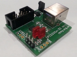
Although I had a quick look to see which PIC microcontroller it was that supported USB, I soon decided that I would have an overall easier time opting for an ARM microcontroller instead. I settled on the NXP LPC11Uxx series of Cortex-M0 chips, as they seemed to be closely related to the LPC1112 I had experimented with a while back.
This article will detail the host PCB for one of these chips, whereas the firmware itself will be covered in a complimentary article.
Circuit design
A large portion of the connections to theLPC11U24 are not strictly required for the purpose of trying out USB functionality, and are included only so that the PCB has some usefulness once I am done with testing — hence the I2C and RS232 headers. Originally I also intended to fan out pin 12 and pins 15-20, but in the end decided that it was worth neither the hassle or the circuit real-estate. The schematic for all the connections to the chip is shown below, where the connections of most interest are the USB and programming-related ones:
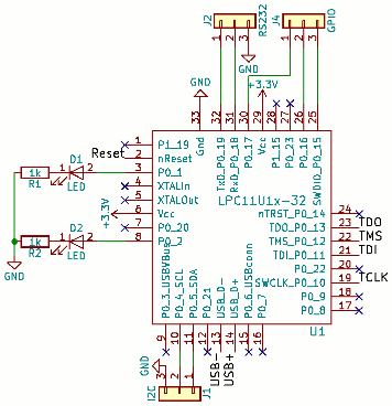
The schematic incorrectly shows LPC11U1x because I was originally going to use an LPC11U14FHI33/201 (the 5mm QFN-33 variant), but since it was out of stock I instead sourced the physically-identical LPC11U24FHI33/301 from the same series. The only difference I was aware of is some extra USB-related features.
USB interface
The whole circuit is powered via USB, and this connection for the USB interface is straight out of the data-sheet. I was not actually sure which USB data lines actually needed pull-ups so I included provision for both — I later found out that which line is pulled up chooses between ‘low’ USB 1.0 speed and ‘full” USB 1.1 speed. The 33Ω resistors between the USB connector and theLPC11U14 surprised me as the FDTI chip I used previously did not require them, and 33Ω is a very low value, but I decided to include them to be on the safe side.
I suspect they are to protect the chip rather than the computer's USB bus.
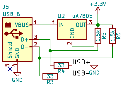
I did have some Mini- and Micro-USB receptacles in stock but I never seriously considered using them — the full-size Type-B receptacle is both more robust and one that I had prior experience using.
As a simplification I decided not to use the USB_CONNECT pin to control the pull-up, as it was only later when looking at the schematic for a development board that I saw that a DTA114Y pre-biased PNP transistor could be used to switch the pull-up in and out.
JTAG interface
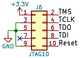
I had trouble in the past with 10-way JTAG connections but since then I ironed out the problems with my infrastructure, and have now adopted a 10-pin MulticompMC-254-10-00-ST-DIP IDC receptacle as my standard connector. Given that there are pins to spare I decided to wire up the circuit for full JTAG rather than just standrard SWD (Serial Wire Debugging) because full JTAG is significantly faster, although I made sure the SWDIO pin was exposed via a pin header so that it was available if for whatever reason I wanted to use it instead.
Opting for full JTAG would turn out to be a mistake.
On-board LEDs
It is always useful having some simple indicators on a PCB for sanity checking, so checking basic things like whether flashing of a firmware is working properly. I opted to use two rectangular through-hole LEDs purely because I had a large stock of them, although they also had the advantage that I can instead slot in receptacles and use them for GPIO. Because I wanted to minimise current draw from the USB bus I originally specced 1kΩ protective resisitors, but in the end used 1.5kΩ because I was already using the latter elsewhere in the circuit.Power header
This power header is attached to the internal regulated power supply. Originally intended as a power output for an external circuit, but in practice used as a power input because often I wanted to power up the circuit but not connect the USB signal lines to my laptop — this is probably not a good thing to do when the chip does not implement any USB functionality, even though it should not result in any electrical damage. There have been one or two times when I suspect Linux completely disabled a USB port due to strange things happening on it, and it took a reboot to reactivate it.
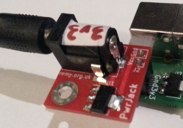
The small red power PCB shown above is something I originally made for use with prototype circuits on perf-board, where including a power regulator is a pain due to extremely limited space. Unlike other mini-PCBs such as my Darlington switch array which were notionally made for convenience but were really experimentation in themselves, this power board has repeatedly proved useful for subsequent projects.
PCB issues
Although the PCB design itself did not have any outright design flaws, there were nevertheless issues that certainly came unconfortably close to causing major headaches, and are detailed in the sub-sections below. Most of these could be put down to having not done any PCB design in the preceeding six or so months, and hence forgotten about potential pit-falls.Landing pads
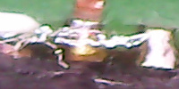
Unlike when I first used a QFN chip for my two-way RF board I did not extend the landing pads, which seriously limited the amount of rework I could do with the chip post-reflow. There were two that looked like it had no solder connection, one of which is shown under magnification below, but attempts to add more solder failed — I suspected neither would be required for USB operation though. Considering all the potential issues I have seen with QFN landings, I will quite likley have to make a customised one for future circuits.
Chip orientation
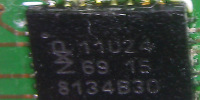
I initially assumed Pin 1 was in the bottom-left corner as it is with the MaximMAX7030, but then noticed a corner dot when viewing under the microscope just after placing the PCB onto the hot-plate for reflow, which suggested Pin 1 was actually the top-right corner. I had previously checked the data-sheet but it did not make any mention of a reference dot, but upon rechecking my suspicion turned out to be right — for future reference below is a magnified image of the chip showing the dot:
Not sure how to fairly root-cause this near-miss beyond flagging up NXP and Maxim for using differing conventions, but QFN markings as a whole are a lot less clear than with other chip types I have used.
Programming track rework
After reflowing I decided to see if my ARM debugger was able to see the the chip, but when I loaded up OpenOCD I got nowt output. By chance when reading the OpenOCD script files I noticed that most of the LPC chips are only supported via SWD rather than full JTAG, which was both annoying but at the same time gave hope that things might still work. Next thing to do was to rework the PCB so that theSWDIO pin was connected to the programming interface instead of TMS — thankfully I had broken out the SWDIO pin to an external header, so after cutting the TMS track it was easy to solder in a patch wire, as shown below:
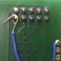
Technically this is really a deficency with the programming software rather than an actual issue with the hardware, but the end result is the same. Once the rework was done the debugger connected fine — had I not broken out the SWDIO pin in a way that allowed such easy rework, I probably would have had to write off the PCB and order a redesigned one.
Bill of Materials
Below is a summary of the components I used to make this board, together with manufacturer part numbers and vendor order codes. Most of this article was drafted before I decided to make such lists a standard part of all my future electronics articles, so it is placed here as an appendix I added just before publication. Only notable thing is that the voltage regulator is from a stock that I bought before Farnell discontinued the part, and the pin header is from a stock I bought off E-Bay where retailers come and go with the wind.
| Description | Manufacturer | Part number | Vendor | Order code |
| ARM Cortex-M0 | NXP | LPC11U24FHI33/301 |
Farnell | 2841069 |
| USB Type-B socket | Multicomp | MC32596 |
1696537 | |
| 3.3 volt regulator | Texas Instruments | UA78M33CDCYR |
discontinued | |
| Red LED | Kingbright | L-113IDT |
2314275 | |
| 33Ω SMD resisitor | Multicomp | MCWR08X33R0FTL |
2447640 | |
| 820Ω SMD resistor?? | MCWR08X8200FTL |
2447726 | ||
| 1.5kΩ SMD resisitor | MCWR08X1501FTL |
2447592 | ||
| 10-pin IDC connector | MC-254-10-00-ST-DIP |
2843527 | ||
| Pin header | Cut from strip bought off E-Bay | |||
| 2-pin receptacle | Milticomp | 2212S-02SG-85 |
Farnell | 1593458 |
Remarks
Considering its experimental nature I think this PCB turned out quite well. Such circuits have an inherant conflict between adding flexibility and avoiding complexity, and in this case the right balance was struck. Putting it all together did not go particularly smoothly, but in the end everything worked. The trickier part was getting the USB firmware working, which will be covered in a future article — below are remarks on things I found out on the circuitry side.- Prototype PCB vs. breakout boards
- Due to the costs and efforts involved, this is one instance where I decided to design a PCB from the outset rather than use a combination of breakout PCBs and prototyping boards. The last instance of me doing the latter turned into a board that was basically wires and receptacles, which has a certain lack of satisfaction — unless components are available in both through-hole and surface-mount form, prototyping on strip-board or perf-board becomes a mess. The purpose of this PCB was to provide a solid base for developing firmware rather than be a project in itself, and since the connections are mainly ones straight out of data-sheets the scope for a schematic error was low.
- USB power
- I now know that USB power is not supposed to be used for direct powering of circuits, and now suspect that this may have been the actual culprit of problems with my USB-I2C adapter that at the time I blamed a bad batch of chips for. This adapter is also the only case where omitting a bypass capacitor rendered a circuit using PIC microcontrollers non-functional, which I now put down to optimism about how ‘clean” USB power rails are rather than sensitivity of the microcontroller chips.
- QFN chips
- They have always worked out well in the end but QFN chips seem to be a magnet for PCB headaches. I suspect they were simply not intended for manual soldering, and I note that the KiCad footprints actually trigger warnings about proximity of pads to each other. On the plus side they seem to be very robust — the first time I did reflow of a QFN I dropped one of the boards before the solder has solidified and the chip pinged off. I put the chip back in place and reheated, and it worked perfectly.
- USB SoftConnect
- On this circuit pull-ups on the USB data lines are hard-wired to the voltage regulator output, whereas ideally it should be software-controlled via the
USB_CONNECTpin. At the time I was not sure whether I could just use a pre-biased transistor, but later on I found the schematic for a development board. - Oscillator requirements
- For full-speed (i.e. 12MHz) operation the system oscillator is supposed to be used, which means using an external clock source. The internal clock I suspect simply does not have the accuracy required. This was a gotcha I only realised after repeated digging through the reference manual cross-checking whether my firmware was doing things correctly.