Darlington switch array
07 November 2017The board is pretty much an array of Sziklai Darlington pairs, albeit with added resistors to limit current, where relatively high-current output is driven by low-current input — this idea came about when I was thinking of replacing the I/O Expander controlled row driver board of my LED matrix display project with direct microcontroller control, which would have required adding in low-side NPN transistors as unlike the PCF8574 I/O expanders PIC microcontrollers don't have current-sinking open collector outputs. I dropped the idea of replacing the row driver board, but went ahead with designing & ordering in the PCBs with the transistor power switches.
As a means to and end this is a second surface-mounted board for me to practice reflow soldering with, even if there was no apparent immediate purpose for the completed board. Being a second-attempt I did a better job of the whole process, most notably making use of a solder mask. I used NPN transistors are pre-biased (i.e. have resistors built in) which saved a bit of space, but at the time I could not find suitably biased PNP transistors, so the board is not as simple as I could have been. I was also unaware of off-the-shelf transistor arrays, but that is all part of the learning process.
Schematic
The schematic of each of the 8 transistor pairs is shown below, alongside the apparent maximum voltage drops for the various components. The upper PNP transistor (BCX17) is the main power switch, which is rated at 500mA, and it is switched on by the lower NPN transistor (PDTD123YT) acting as a current sink. With the row driver within my LED display project the I/O Expanders were open-drain that acted as current sinks for the high-side PNP transistors, but in this schematic the NPN transistors convert Ground/Vcc voltage signals expected from typical microcontrollers into the high-impedence/current-sink required by the PNP transistor base terminal.
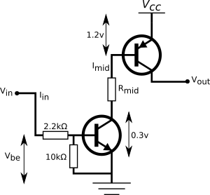
The Vbe of the lower NPN transistor is unclear from the data-sheet, but it seems to have a switch-on current of 0.65mA, which with a gain of 70 would allow a collector current of 45mA — as will be seen later this is vastly in excess of requirement. For this current Vin-Vbe needs to be at least 1.43 volts, which I have no doubt will be the case in a 5-volt circuit. At 300mA output the gain of the upper PNP transistor is 70 which requires a base current Imid of 4.2mA, and for 500mA the gain of 40 requires 12.5mA — the graphs indicate the latter is actually a corner-case with very low temperatures. Not wanting to stress the transistor I will target Imid of 5mA. The maximum emitter-base of the upper PNP transistor seems to be an unusually high 1.2 volts, and the the saturation voltage across the lower NPN transistor is 0.3 volts, which means the voltage across the inter-transistor resisitor is 3.5 volts. I opted for a 680Ω resisitor for Rmid which would allow a current Imid of just over 5mA to flow — however given that calculations used edge-case data-sheet values I would not be surprised if in practice 1-2kΩ could be used. Since the other resistances are built into the lower NPN transistor package, the only real variable is the value of Rmid, and its only real task is to avoid a wastefully-high current Imid out of the PNP transistor base. Unlike the typical Darlington/Sziklai this is intended as a switch rather than a high-gain amplifier, even though it is taking advantage of the high gain.
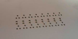
Solder stencil mask
Putting down the solder paste I think is the one part of reflow soldering that is the most tricky, but this time round I made use of a solder stencil that greatly simplified the process. A solder stencil is a mask that is placed on top of the PCB, and then solder paste is simply spread over the top of it — the holes in the mask mean that each pad will be covered by the ideal amount of solder paste. Try to avoid getting the solder paste on your fingers as it is difficult to get off, will leave your fingertips feeling a little rough, and in any case quite likely contains toxic stuff such as lead (don't do reflow soldering this just before eating). The mask I used for this PCB is shown below:-
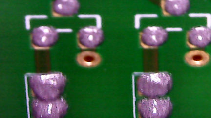
Quite a bit of the solder paste will likely go to waste, and it will also be a lot messier as the paste will be smeared all over the mask when you have finished, but it is a lot quicker and easier than putting paste on all the pads by hand. I did have a solder mask for my previous SMD PCB, but I had not constructed a board to hold everything in place while I spread out the solder paste. With a mask the component pads are covered close to exactly, as shown on the left-hand image below. Once done I put on the components, as shown on the right-hand picture.
I was not keeping close track of time, but I think the whole process of putting down the solder paste and placing the components took about 10 minutes. It is best to put a component down on the paste in one quick move, and only trying to move it around if it is vastly out of place — I found that trying to give a component a slight nudge more often than not dislodged it completely.
Reflow heating
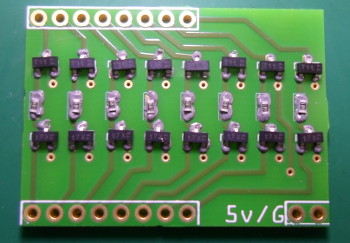
This time round I put a 5mm steel plate on top of the hot-plate to spread out the heat, rather than putting the PCB directly on the hot-plate itself, and it also had the effect of slowing down the speed at which the board was heated up — using an infrared thermometer to check the temperature solder reflow happened when the components were at 180°C, although the hot-plate itself was around 230°C long before this point. I think an Aluminium plate would have been better due to lower specific heat capacity, but results would probably have been much the same. When reflow was finished, the board looked like below:
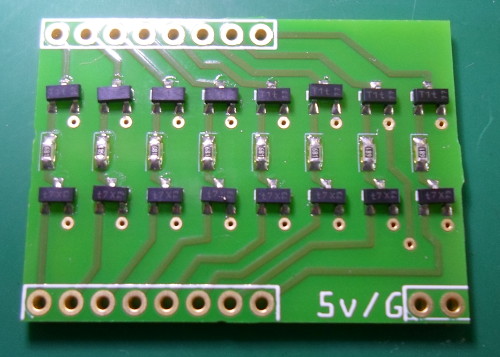
The outcome is visually a lot better than the resisitor arrays — the transistors are not perfectly straight but all of the resistors are, and more importantly all of the solder joints look good. I did a quick check of the latter using a microscope, and most of them looked perfect to me. However the real factor is whether things work properly rather than look good.
Testing
To test the PCB I used the simple breadboard circuit below, with power provided by a 5 volt regulator supplied by a 9 volt power cell. The inputs were connected to Vcc (i.e. 5 volts) and the outputs connected to LEDs using my previously-created resistor array to provide protective resistance. This was intended as a basic “smoke test”, and I did not go as far as checking whether the current flows were the values expected from the previous calculations
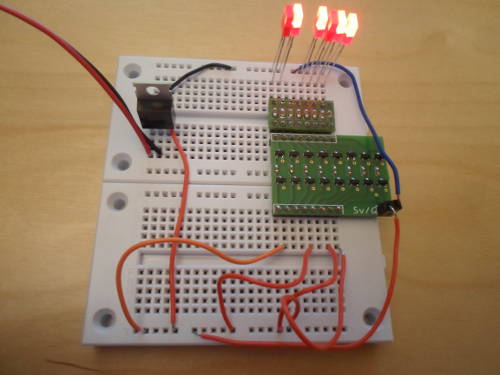
Although not shown in the picture, all eight transistor pairs operated as expected first time, so there was no need for rework on the PCB. I had no reason to expect faults, but given the complexity of the circuit and the relative inexperience with the methods, it was nice that it all just worked.
Remarks
Reflow soldering is a very different ball-game compared to through-hole PCBs, but as was the case with the latter I actually found it not that difficult and with universally good outcomes. I originally looked into reflow soldering because I had some chips that are not available in through-hole packages, but after this experience with SMD PCBs, I can foresee ordering in SMD boards in preferance to through-hole PCBs. At first the realisation of the size of SMD components only really sinks in when they arrive, but this soon gives way to the surprisingly fast turnaround time. These points, alongside others, are briefly discussed below.- Scale
- I tried to choose “big” components, but SMD sizes are a different order of magnitude to through-hole components, and within CAD programs (read: Fritzing) it is easy not to realise scale. Resistor pads are quite big, but everything else isn't. A follow-in surprise is that the small scale is not really a difficulty, with magnification actually makings things harder rather than easier.
- Speed
- Even my very first board, which would have taken longer than usual, did not seem to take very long to process — and the second one I did shortly afterwards probably only took between five and ten minutes all-in. I think soldering up a comparable 24-component through-hole PCB would take best part of an hour, but this power-board only took about 10 minutes.
- Working first time
- Perhaps a bit unfair as my through-hole PCBs have also worked first time, but these previous boards were both simpler, and would have been easier to correct. The one failure was when I was really trying push what I could get away with, and it was still easily repairable.
- Cost
- SMD components are designed for bulk-buying, and are a lot cheaper than equivalent through-hole packages. Often the minimum order is 50 or 100 units, but this often works out as only a Euro two. As for PCBs, the smaller size also equals lower cost, although this is offset by the cost of getting the solder paste mask.
- Selection
- The selection of components available only in SMD packages is surprisingly big. I was not aware of them at the time I ordered in the PCB fabrication, but since then I became aware of transistor array chips such as the ULN2003ADRG3 and ULN2003D1013TR, which in hindsight may or may not have been a better choice of component.