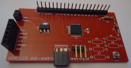
LCD dot-matrix display, 2nd gen.
13 October 2019This PCB is a reimplementation of my previous LCD dot-matrix display using an ARM Cortex-M0 chip. While the Microchip
PIC16F1828 used on the previous generation curcuit was adequate for working out how to use the LCD panel and getting things displayed, the limited amount of RAM that is also fragmented across multiple banks means it was not suited for anything much beyond display of graphics generated elsewhere.
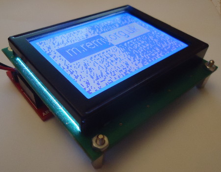
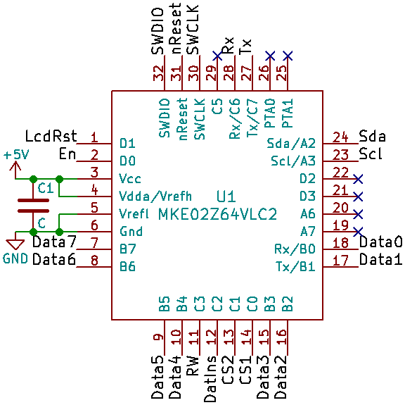
This redesign uses an NXP Kinetis E series MKE02Z64VLC2 (Farnell 2345460), which unlike other ARM microcontrollers I have come across in the past, is capable of running off a 5-volt power supply rather than being limited to 3.3 volts. Although this is the third ARM based chip I have tried out, it is the first that I have used to implement a practical circuit rather than just experiment with — at time of writing I have yet to write the MAC firmware for a bi-directional RF control circuit I designed last year, and so far I never did anything beyond some GPIO with the Cortex-M4 bootstrap PCB.
The circuit
Most of the circuit is connections between the microcontroller and the header for the LCD display, the schematic for the latter which is shown below. The main divergence from the LCD display data-sheet is the LCD back-light power connections — from experimentation I worked out should be connected to the 5-volt power rail in series with a 120Ω resistance, the latter value being an effective brightness control.
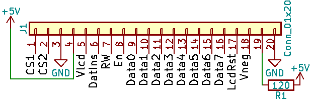
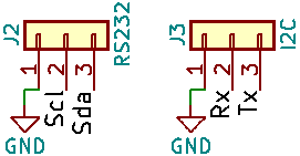
Due to the nature of the circuit the PCB is also a de-facto breakout board for the MKE02Z64VLC2: The 20-pin header for the LCD display connection includes 13 GPIO pins — including all eight of Port B and four contigious ones from Port C — which is more than enough for anything I am likley to need on a prototype board. Also included on the PCB are seperate RS232 and I2C headers as well as the JTAG interface, so in total 21 of the 28 functional pins are exposed. The corresponding microcontroller schematic can be seen below; the matching of LCD display pins to chip pins were chosen to aid writing of the firmware.
Bypass capacitor
I was not sure if a bypass capacitor — also known as a decoupling capacitor — between the power pins was required, as a quick search of the data-sheet did not mention them, so I decided to provision for one just in case. In practice I have only had one instance in the past where a circuit did not work until I had put a by-pass capacitor in place, and for this circuit I ended up omitting it. I consider is good practice to include a bypass capacitor, although of all the PCBs in my latest batch this is the only one that actually included one.Contrast control
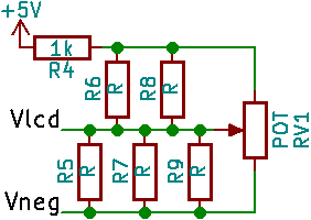
When I built the original circuit the least clear thing was the purpose of theVlcd pin, which I eventually worked out was for contrast control. That it was supposed to be powered via a potential divider placed between Vcc and Vneg was pretty much only mentioned in passing by the data-sheet. In practice I found that it needed to be set very much towards Vneg in a ratio of around 20:1. For flexibility I provided both a resistor network and a trimming potentiometer.
Data connection headers
As with the original circuit I have included both RS232 and I2C connections, and unlike the original the RS232 connection includes both receive and transmit lines — previously I omitted transmit as it was not strictly required and I was needed the extra pin for the display header. I did consider having RS232 voltage levels, but lack of space for a D-sub connector and the cost of voltage driver chips discouraged it.
JTAG connector
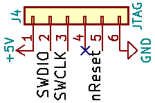
For this circuit I decided to try out my previously untested custom 6-pin connector, for which the schematic is shown below. For some reason the Kinetis E only supports SWD (Serial Wire Debugging) programming rather than full JTAG, which is the use-case that my connector was made for. I only used a six-pin header rather than a five-pin one due to having a large stock of the latter for use a PIC microcontroller programming interfaces.
Power supply
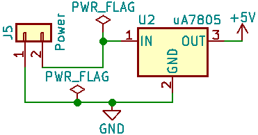
For the on-board power supply I used a Texas InstrumentsUA78M33CDCYR, which is a 3.3-volt SOT-223 low-drop-out voltage regulator I bought a large stock of late last year, and the schematic of this together with the external connection for the unregulated power connection is shown below — the PWR_FLAG symbols are required to suppress warnings in KiCad regarding undriven power pins. Nothing special here as the majority of the circuits I build include some form of power regulation.
The PCB itself
These days when I order PCBs I normally include between three and five different designs in the order to amortise shipping costs, and this board was originally included to pad out a multi-design order due to a special offer being in place. However it was one of two designs that made use of a new chip, and due to its relative simplicity — it only needed basic GPIO and some timing, and would be a self-contained project — it ended up being the first to be used.
Through-hole resistors
Although the range of SMD resistors I have is growing, it is still not anywhere near as extensive as my collection of through-hole resistors, so in designs like this that are not space-constrained I still make use of them — I made a similar decision with my LCD timer control board. A secondary concern is that I might end up trying different combinations of resistances, and I feel that through-hole is a better choice for quick adding and removal of components.Choice of flux
Originally I got a bottle of EdsynFL911 flux but anecdotally this was a bad choice as I got much better results when I later switched to using a Circuitworks (now Chemtronics?) CW8100 flux dispenser pen. I am not sure whether it is due to a different flux formula, the different way the flux is applied via pressing rather than a brush, or whether the switch-over simply coincided with other factors — I found a dispensing pen a lot more convenient so never did any controlled experimentation.
Experience soldering QFP chips
TheMKE02Z64-VLC2 is a 7mm LQFP-32 which although is not the first QFP chip I have used, is not really comparable to the 100-pin LQFP Cortex-M4 I reflow soldered around the same time last year. The nearest comparable chip is the SSOP-28 Cypress I/O expanders which I suspect I hand-soldered at least some of, but compared to my generally unfavourable memories hand soldering of SSOP & TSSOP chips the LQFP-32 actually went quite well. In hindsight the LQFP-32 was not pushing my ability anywhere near as much as making the 17-segment LED modules did, with the pin pitch of 0.65mm versus the 0.5mm of TSSOP providing a small but critical amount of relative slack.
Firmware
The firmware for the Cortex-M0+ on this board, which is available from my Bitbucket account, is a reimplementation of the PIC-based firmware code used for the original control board, and the issues discussed previously still apply. At time of writing only the GPIO needed for controlling the LCD display has been written, although I plan to extend the firmware to include external communications via the serial interfaces, but such firmware implementation details are beyond the scope of this artice. There is another circuit based on the same ARM chipset in the pipe-line, and I plan to discuss more general firmware issues in a future tech section article once this latter circuit has been completed. The following sub-sections discuss firmware-related issues that I feel are best addressed in this article.Pin allocations
With the previousPIC16F1828 based control board all eight of the data lines were allocated to Port C, as it allowed the data lines to be treated as a single eight-bit variable, and enable was on its own on Port B since it would be toggled separately. On the QFP-32 MKE02Z64VLC2 all of the available GPIO pins are accessible through the same 32-bit register, so the separation of GPIO pins into ports does not have the same importance. However due to Ports A4-5 and C4 being used for programming all possible contiguous eight-pins will overlap with Port B, so for simplicity all Port B pins were allocated to data lines. Of all these pins only PTB4 does not default to GPIO, so this latter pin will need to be reassigned.
Drawing buffer
The firmware for the originalPIC16F1828 based circuit was not much more than a thin I2C-to-parallel conversion layer, whereas the firmware for this ARM-based board includes a drawing buffer that is copied to the LCD display. This allows higher-level rendering to be off-loaded onto the control board, which was not realistic with the previous board. The buffer uses an array of 64-bit integers, where each integer represents all the pixels over the eight rows in each column.
Flashing speed
One notable thing is the speed that firmware can be flashed to theMKE02Z64VLC2, which is a lot faster than with the NXP LPC11(U)xx family. Looking at the OpenOCD target scripts this is because the script for the latter assumes a ”real slow” default of 10kHz just in case any boot loader is doing screwy things with the system clock, whereas for the MKE02Z64VLC2 it just uses 1000kHz. In practice this means flashing taking a second or so rather than half a minute, the latter which quickly gets annoying. I suspect I could bump up the speed as for now I am not interested in fancy bootloaders or clock manipulation. Beforehand I thought the slow speed was simply an inherent thing with SWD.
Watchdog pains
After much banging of my head against the table wondering why some very basic LED blinking code was behaving strangely, especially when being examined via GDB, it suddenly occurred to me that a reset watchdog might be tripping. The hunch was right, but the process of disabling the watchdog on aMKE02Z64VLC2 chip uses a procedure for which the chipset reference manual is both unclear and incomplete — it involves entering a special unlock code, and then setting several parameters some of which the need for are unclear to me. The sequence below I scratched together based on several sources — I forget which ones were most helpful — and some experimentation:
REG16(0x40052002) = 0x20c5; REG16(0x40052002) = 0x28d9; REG8(0x40052001) = 0; REG16(0x40052004) = 0xffff; REG8(0x40052000) = 0;
All other ARM chipsets I have used have any watchdogs disabled by default and my boilerplate PIC firmware headers explicitly disable them, so it has been a long time since I last had to deal with the pit-falls. I am skeptical as to their true value because having to make sure the watchdog of check-pointed opens up a whole surface for bugs. Making them enabled by default and difficult to disable is particularly irritating — I am doubtful of the firmware screw-up cases where such protections would be useful.
Bricking the chip
I have to call this out: The Kinetis E series of microcontrollers are far too easy to inadvertently brick — I did this with one of them and came alarmingly close to doing it to a second, and the sub-sections below detail where these pit-falls are. The underlying problem is positioning of options in a way that invites inadvertent changes while in the process of configuring other things, coupled with making most combinations of bit patterns triggering activation rather than deactivation.Reassigning non-GPIO pins
Three of the four pins that do not default to GPIO instead default to functionality related to firmware flashing, but the fourth defaults to interrupt and since it is in the middle of GPIO Port B, it needs to be reassigned. This is done by writing to register0x40048004, but this has to be done with care. I accidentally put in 0xc0 rather than 0x0c, so rather than just changing the interrupt pin to GPIO, I also changed the reset and SWDIO pins. This resulted in a chip that could not have anything else flashed to it, and since the firmware was incomplete the chip was effectivly bricked.
I think there are ways to unbrick the chip via a factory reset, but I have yet to work out how to do this. It involves power cycling while the reset pin is shorted to ground and then doing a bulk erase, but at the very least this would mean bypassing some of OpenOCD's usual sanity checks. It was quicker and easier to solder up a new PCB, and work out what to do with the bricked one another time.
Flash protection bytes
The 16 bytes within the flash address range0x0400–0x40f contain security information that is loaded into read-only registers on reset, and these provide fairly fine-grained levels of protection of the flash contents. Originally I did not account for these in the stub and linker scripts, and most of the combinations of the relevant fields put the chip into a secured state that require a bulk erase to unlock. This was annoying but it could have been a lot worse — I later found out that bulk erase itself can also be disabled, and it was pot luck I did not hit these bit patterns. I modified my stub code so that, assuming I read the reference manual correctly, all protection is disabled by default.
Impressions of the Kinetis E
This Kinetis E KE02 was a chip I chose because it was made by NXP, but it soon transpired that it was designed and produced by Freescale Semiconductor before the latter was subsumed into NXP, and hence very different from the NXPLPC11xx series I had used in the past.
I very quickly got the feeling that the documentation assumed previous experience with other ARM-based components, and various gotchas such as the watchdog timer make it a lot harder to get up-and-running than other chips out there, so this is not the chip to use when figuring out ATM stuff for the first time.
There are not many 5-volt tolerant ARM-based microcontrollers out there to begin with, and of these only a fraction seem to have OpenOCD support, so the Kinetis is basically the best of a bad bunch — the Infineon XMC1x00 series is the only viable alternative I have seen so far, although it looks like it also requires a bit of messing around with flash-stored configurations that could also brick the device.