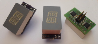
17-segment LED module
10 August 2018This mini-PCB is a breakout board for the
PSC05-11xxxxx series (Farnell: 2373487 - Green; 2373489 - Red) 16/17-segment LED chips, which reduces the number of interface pins from 18 to 8. It is essentially the 5-to-17 expansion used on the 17-segment LED display shrunk down so that it fits on the underside of the LED chip, so it is an active component rather than just a passive connection routing board like the LED matrix modules recycled for the previous circuit.
This PCB is not the first I have made to have components on both sides, nor is it the first to make use of TSSOP components, and being only two-layered it is not even the most complex in terms of track connectivity. However it was nevertheless pushing my abilities due to the density of attached components, especially since I decided to forego getting a solder mask and hand-soldering the boards, with the whole experience having a higher-than-usual rate of mistakes for recent projects.
Motive
With LED displays a significant part of the circuit logistics is wiring up the segments, and the 17 that thePSC05-11xxxxx have mean that wiring up a circuit to use these LED chips is a project in itself. In the past designed a PCB that contained multiple 17-segment LED chips, but I felt that the result was an expensive alternative to using an off-the-shelf LCD display — in hindsight its fundamental fault was that it just turned a wiring problem into a PCB track routing problem. I later decided that the only approach that made sense was having a single LED chip per breakout, much like the LED matrix modules used in the matrix display circuits, as the solution was to substantially reduce the number of pins each chip required, rather than using a PCB to off-load the problem of connecting several up.
Simplified circuit overview
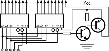
The core part of the circuit is two 3-to-8 decoders and a transistor pair, shown in the schematic below, which together act as a 5-bit to 17-bit parallel expander. This was previously used as a way to reduce the number of microcontroller pins required to select the segment to enable, and here it is used to reduce the number of connections needed for each LED chip on a host circuit board.
My hunch was that the smallest form-factor of components used to drive the segments within the previous 4-character display could fit on the underside of the LED chips, and if it could be pulled off the number of external connections needed for segments could be reduced from a logistically-difficult 17 down to 5 — 4 if the decimal point is omitted — which would be relatively easy to deal with.
Component selection considerations
The original intention was for the module board to have the same area as the LED chip, which meant all the other components needed to fit in the space between the mounting holes. In practice there was not quite enough space, so I decided to put the transistors on the same side as the LED chip, which was as much about aesthetics as available space. From the outset I decided to hand-solder all components rather than using solder paste, because for components of this size rework would be hard to avoid in any case, and I wanted to avoid the messiness that comes with reflow soldering.Surface-mount header pins
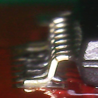
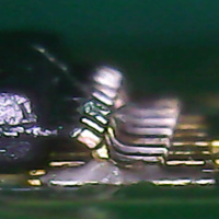
A major headache with the LED matrix modules and the column driver host board they plugged into was track routing problems caused by the mounting holes for the pin headers & receptacles. In both cases they divided the board into two, preventing tracks running north-south. For the 17-segment LED module to be viable, tracks would have to overlap with the area occupied by the header pins, which meant using surface-mount interface pins that only occupy one side of the PCB. The one problem with these is getting alignment right, as demonstrated in the picture below:
This misalignment is because surface-mounting does not guarantee alignment in the same way as through-hole components do, but the extent the above example is out of alignment is down to not quite having worked out the right technique for soldering these headers.
3-to-8 decoders vs. 4-to-16 decoders
When I was initially looking at available decoders, I noticed that the selection of 3-to-8 decoders was much better than 4-to-16 decoders — most of the latter were the inverting type where the address selects the output pins that is low (i.e. all other pins are hi) rather than the non-inverting type (i.e. all but selected pin low) that at the time I considered more useful, and they were available in less form-factors. As a result I never seriously considered using a 4-to-16 decoder rather than two 3-to-8 decoders — TICD74HC238PW (Farnell 1741523) — and from the tight squeeze it was to get all the PCB tracks in using two of the latter, it possibly was a good decision to not even try.
The dot transistors
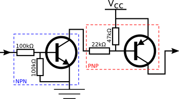
As with the 4-character 17-segment LED display that the LED module is based on, a Sziklai pair of transistors — an arrangement used in the Darlington switch array daughterboard — is used to provide the extra output that the two decoders cannot accommodate. The PNP transistor that supplies the dot segment is aPDTA124XT (Farnell 8736898), which is the SOT-23 version of the PDTA124XU that has been experimented with previously — at 5 volts this 22kΩ/47kΩ biased transistor supplies a maximum of 50mA, which was ideal considering the maximum DC current of the LED chip is 30mA. The NPN transistor that is attached to the PNP base only has to sink a current of circa 0.2mA, so a DTC115ECAHZGT116 (Farnell 2769605) was used purely for its very high bias values of 100kΩ/100kΩ. The schematic below summerises the transistor pair, complete with all the bias resistances.
Segment addressing
The pairing of decoder output pins and LED anode (positive) pins were chosen purely to ease track routing on the PCB, so the address that each segment gets — which are listed in the table below together with a figure showing the segment identities — is basically random. The one exception is the decimal point which was deliberately assigned to the transistors rather than being powered via a decoder pin, and hence has the address0x10. This is intended to allow 4-bit addressing in the cases where the decimal point is not required.
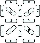
| Segment | F | G | T | S | R | D | E | U | B | N | C | P | K | M | A | H | . |
| Address | 0x00 |
0x01 |
0x02 |
0x03 |
0x04 |
0x05 |
0x06 |
0x07 |
0x08 |
0x09 |
0x0a |
0x0b |
0x0c |
0x0d |
0x0e |
0x0f |
0x10 |
Segment testing
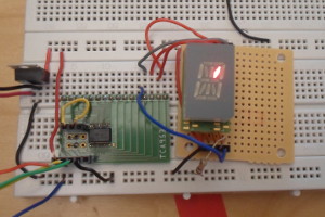
To test the segments a basic breakout board is used so that the LED module can be wired up to aTCA9535 I/O Expander, with the LED module address pins being assigned to expander I/O port in order of increasing significance. There is nothing special about the choice of I/O expander — it just happened to be one I had close to hand that was a convenient to slot into place. The test circuit is shown below:
The expander is controlled using the USB-ISS I2C master. Below are the required command-lines for the setup of the expander and choosing which segment is lit — see the article describing the expander for details on these commands.
~/bin/i2c-tty-setup.exe ./ttyTxRx.py /dev/ttyACM0 1 55 40 06 1 0 ./ttyTxRx.py /dev/ttyACM0 1 55 40 02 1 <addr>
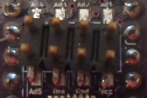
Pin ordering
The table below shows the module interface pin ordering from the top-down view of the receptacle the header is intended to plug into. Main thing to note is there are two grounding pins — there is theGround pin which is the Vss connection for the decoders and transistors, and there is the Drain pin which is the common cathode of the LED chip. The latter should be connected to ground via an appropriate current-limiting resistor. If the decimal point is not going to be used, Addr.5 should be tied to ground.
| Addr.1 | Addr.2 | Addr.3 | Addr.4 |
| Vcc | Ground | Drain | Addr.5 |
Soldering
For circuits such as this with relatively few components, my preference is to hand-solder surface-mount components rather than using hot-plate reflowing. Reflowing with decent solder paste gives much better results, and in particular rework goes much more smoothly with a low-temperature paste such as Chip QuikSMDLTLFP (138°C, 42% Tin, 57.6% Bismuth, 0.4% Silver), but overall dealing with solder paste is much more hassle — cleaning solder stencils with fine apertures is a particular pain, and the whole reflow process needs a large block of time to be set aside to get everything done in one go. Hand soldering has a higher botch-rate but this is offset by the cost of solder masks & paste, and when only doing one or two boards rather than several it is also significantly quicker. Since the LED module PCB is double-sided, reflow soldering was not viable in this case anyway.
Choice of soldering tip
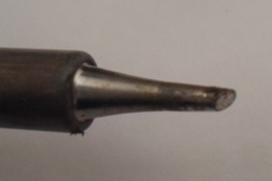
For hand soldering of surface-mount components, and in particular the removal of solder bridges, it helps a lot to have an iron tip with a flat hoof rather than a pointy end. Compared to the standard Hakko tip, theT18-C2 (shown below) has a much larger surface-area for the transfer of heat, and it makes the most difference when using desoldering braid. Unlike the pointy tips, the flat hoof has a decent flat surface for the transfer of heat, and I noticed the difference it made almost immediately.
This tip is an utter pain for through-hole soldering though, which is awkward for a PCB such as this that has a mix of surface-mount and through-hole components, so I ended up buying a second soldering handset to avoid having to keep change the tip.
TSSOP vs. SSOP chips
On the PCBs ordered from Seeedstudio that used one SSOP & one TSSOP chip rather than two TSSOP chips, I found that the SSOP chips were slightly easier to deal with, although this is somewhat anecdotal as it might be influenced by doing the TSSOP chips first and then doing the SSOP chips. The pin pitch on both form-factors is almost identical, but the SSOP chips have almost twice the height at the point the legs go into the chip itself, and this extra height might be helping where the solder ends up. In the picture below, the red PCB has a SSOP chip whereas the green PCB has a TSSOP chip:
The TSSOP landing pads went further under the chip than the SSOP landing pads, but I am unsure whether this was the source of any problems, as the pads were actually shorter than those recommended in the data-sheet. I suspect that I could have tried soldered TSSOP chips onto the SSOP landings, but it would have been a very tight fit.
Ordering the PCBs
I am unsure whether it was an original intention to compare the two form-factors or a complete accident, but the Gerber design files submitted to Seeedstudio had one TSSOP and one SSOP landing pad, and by the time I realised this it was a few minutes too late to amend or cancel the order. For some reason Farnell don't stock the SSOP variant of the74HC238, so I decided to submit a corrected design that used two TSSOP chips to OSH Park and Aislier, in part so have an all-thing-equal comparison of the three fabrication services. I was later able to source some SSOP variants from Digi-Key, so the Seeedstudio boards did not go to waste. The costs and lead times are summerised in the table below:
| Foundry | Ordered | Factory | Shipped | Arrived | Price | P&P | Unit cost |
| Aisler | 30th June | 2nd July | not stated | 12th July | €5.70 for 3 | Free | €1.90 |
| OSH Park | 30th June | 5th July | 11th July | 25th July | $3.70 for 3 | Free | €1.05 |
| Seeedstudio | 30th June | 4th July | 9th July | 23rd July | $4.90 for 10 | $12.24 | €2 |
With Aisler you are paying for the fast turnaround time — order on the Monday and you should have the PCBs by the weekend the following week. From past experience Seeedstudio has a very consistent order-to-arrival time of between three and four weeks, so the time to arrival in this instance is at the quick end of my expectations. They provide a detailed order progress report, although I am suspicious as to its accuracy because some of the legs — most notably prior to departure from Hong Kong airport — have a lot of variance which does not affect overall lead time. OSH Park was somewhat disappointing this time round, but I suspect this may be due to the treatment of US Postal Service items once they leave the US.
Remarks
The only thing I regret about these LED modules is that the LED chips cannot sit flush next to each other, but otherwise I got what I set out to achieve, even if the process was a little bumpy. Component clearance and the overall tight fit of the circuit was a challenge, in particular there being no room for rework once the pin headers were in place, but these were not insurmountable issues. The basic decision to use chips I could squeeze in between the LED chip pins, and the use of surface-mount headers that did not penetrate the PCB, were spot-on. The mountings for the LED chips should have had a lot more flange and a bit less hole, and the choice of resistive biases for the transistors may cause issue with lower circuit voltages, but these are not critical issues.If I was to redo this module from scratch, I would dispense with the decimal-point and design a module that only required six header pins — this would include an on-board current-limiting resistor but would dispense with the transistors. This is a big trade-off, but the decimal-point seems less important for display module intended to show text rather than just digits. I might also try using just a single 4-to-16 expander and move the header pins away from the centre and/or in a different orientation.