SOT-323 transistors
24 March 2018When I was designing the Darlington switch array a few months ago I took note of SMD transistors that were pre-biased, which meant that they came with built-in resistors, and used one such transistor — the NXP
PDTD123YT (Farnell 1510760) — as the NPN part of the transistor pairs within the array. My use of NPN transistors in circuits is as current-sinking switches, and a combination of the gain and the internal resistances dictates how much current can be sunk. Having stocked pre-biased transistors with a range of gains and resistances, it was about time I evaluated the current ranges they were suitable for sinking.
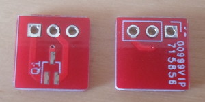
This article contains the evaluation of several SOT-323 size pre-biased transistors I have stocked, and since SOT-323 is a surface-mount component size, I ordered in some custom break-out boards that allow these transistors to be put onto standard 0.1 inch (2.54mm) solderless breadboard. Part of this article covers the experience of getting these breakout boards fabricated. On the PCBs the landing pads for the transistors are extra-wide to (supposedly) aid hand-soldering. The transistors are listed below:-
| Manufacturer code | Farnell code | Headline gain | Max current | Base Ω | Ground Ω |
PDTD113ZU |
2469726 | 70 | 500mA | 1k | 10k |
PDTC114YU |
8737070 | 100 | 100mA | 10k | 47k |
PDTC124XU |
8737215 | 80 | 100mA | 22k | 47k |
Breakout board fabrication
For this board I decided to use Seeed Studio PCB service, in part to see what they are like. Their pricing is somewhat non-linear, and for a 1cm-by-1cm board — the minimum size the foundry accepts — is somewhat biased towards bulk orders, with the difference between 15 units and 40 units being only 49¢. I opted for 30 as this number was already vastly in surplus of what I needed, and this came to $19.94 plus $12.32 delivery, which works out at $1.07 each. For comparison Aisler worked out at €1.90 ($2.34) each, including delivery. Pre-ship lead time was a stated 5-6 days, but with the Chinese new-year shutdown I knew it would be a few days before they would even started on the order, and there would probably be a back-log. Therefore I decided it best to omit commentary on actual lead time.
Delivery was via something they called EU Post (in reality it was handled by Royal Mail) which I think had a stated shipping time of 12 or so days, and in practice took 17 days from the date that shipping was supposedly dispatched on — to be fair 6 of those 17 days were between it arriving in London (air freight via Hong Kong) and it turning up on my doorstep. Although supposedly significantly faster DHL and FedEx courier shipping were also offered, the order form insists on a VAT/EORI number for them, so I was unable to use them. From memory they were around $20, which was not that much more than the postal option I ended up using.
Doing the soldering
I had opted PCB footprints that were intended for hand-soldering, and given that SOT-323 was that bit smaller than I expected, it was just as well I did. I think the hand soldering would have been somewhat easier had I used a smaller soldering tip, as one of the transistors had a broken connection — I suspect the leg itself was not heated, so the solder did not stick to it. Unlike when I was previously hand soldering SMD resisitors a microscope is required, as the landing pads are still quite small compared to resistor footprints. Although there is not much size difference, in hindsight I should have ordered SOT-23 rather than SOT-323 form-factors for all, as the former is about 50% wider. This means that the two legs that are on the same side of the chip have that little extra space, which helps if using an over-sized soldering iron tip. SOT-23 is also that bit easier to see, and that bit less likely to ping away when removing it from the packaging.Load testing
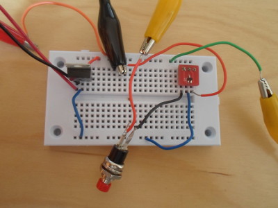
I tested three scenarios with the mounted transistors: Open collector, a power load consisting of an LED in series with a 390Ω resistor (a stock component pair), and the collector connected directly to the positive power rail. The last of these three circuits is shown in the picture below. I used my analogue multimeter to measure the collector current and my (much more accurate) digital multimeter to measure the base current. I also included a button because such a setup is one that will draw a lot of power and should only be active long enough to get current readings.
The resulting current readings are shown in the table below. Those under direct connection correspond to the test-case where the collector is connected to the positive power rail, and is supposed to represent the maximum current the transistor is able to sink. Because of the accuracy of the analogue multimeter the collector current figures are rounded to one significant figure. The supply Vcc was measured as 4.95 volts.
| Manufacturer order code | Base current | Direct connection | |||
| Open collector | 380Ω (7.85mA) | Base current | Collector current | Effective gain | |
PDTD113ZU |
4.75 | 4.7 | 0.82 | 200 | 244 |
PDTC114YU |
0.46 | 0.45 | 0.40 | 70 | 175 |
PDTC124XU |
0.19 | 0.18 | 0.18 | 50 | 278 |
With the PDTC114YU and especially the PDTD113ZU cases it is pretty clear that the power supply was struggling, to the point that I suspect that ZU is actually capable to sinking substantially more current — to me it looks like the base current is actually being limited by the collector current rather than the other way round as expected. As for the PDTC114YU transistor the 70mA it passes looks plausible, and since it has a maximum rating of 100mA would probably not want to try drawing much more than that through it in a real-world circuit. The 50mA that PDTC124XU passes I am prepared to accept at face-value, particularly as the effective gain matches up with the 25°C DC gain graph in the data-sheet.
Matching the data-sheet
The next question is whether the values obtained above could realistically be derived from the data-sheet, and since it is the one transistor that did not have any apparent power supply issues, I will consider thePDTC124XU first. Its base current of 0.19mA across 22kΩ implies the voltage drop of 4.18 volts, which is 0.77 volts less than the supply Vcc — not far off the typical base-emitter drop expected of a typical transistor, and close to VI(On) of 0.8 volts quoted in the data-sheet. However the same calculation for the other two transistors does not match up so conveniently, suggesting a lower base-emitter voltage drop, but the built-in resistors mean that the probing required to tell for sure cannot be done. For the PDTC124XU transistor the experimental gain of 278 is close to what the 25°C plot on the DC current gain chart suggests it should be, whereas for the other two it is between the plots for 25°C and -40°C — this effective de-rating is quite plausibly also down to the aforementioned power issues. My prior assumption would be to use whatever gain corresponds to a collector current of 10mA at 26°C, which results in somewhat conservative values.
Conclusion
ThePDTC124XU transistor was one I selected because it had a very high built-in base resistance, so I am not surprised the current flow it permitted was half its maximum rating, but for the other transistors I suspect they could be maxed out within a 5-volt circuit. For the other transistors I suspect part of the problem was also having to dissipate the power as well, so I was hitting a power limit rather than a current limit.