SN74HC161N binary counter
28 April 2018When using LED chips — either segmented displays or dot matrices — there is typically one set of inputs that are powered in a fixed round-robin order, and in the ideal case all that is needed from the display controller is a signal indicating when to switch to the next power line in sequence. I did manage to find a chip that actually did this, but it was a low-volume legacy chip that sold for about €10 each, and I did not want to go down the road of programming a microcontroller to do the same task.
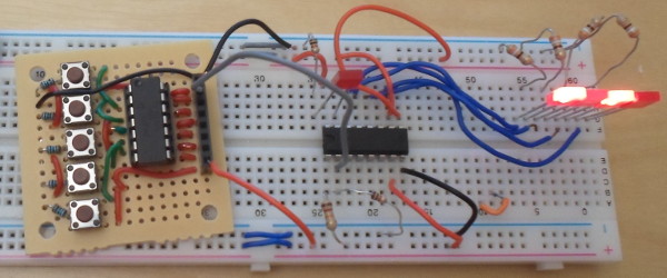
The Texas Instruments SN74HC161N (Farnell 2407119; datasheet) is a 4-bit binary counter, which when combined with a binary decoder such as the 74HC238 which expands binary out, provides a way for a single signal line to control the activation of parallel power bus. Had I known about these chips earlier, several of my past circuits would have been designed differently.
Pin-out
The counter data-sheet dates back to 1996, a time when presentation was somewhat different and it seems certainly less exhaustive, and the table below summarises what I worked out from reading it:
| Formal name | Vcc | RCO | QA | QB | QC | QD | ENT | LOAD |
| Purpose | Vcc | Maximum | Binary output | Enable T | Load | |||
| Pin number | 16 | 15 | 14 | 13 | 12 | 11 | 10 | 9 |
| Pin number | 1 | 2 | 3 | 4 | 5 | 6 | 7 | 8 |
| Purpose | Clear | Clock | Load input | Enable P | Ground | |||
| Formal name | CLR | CLK | A | B | C | D | ENP | GND |
Unusually the data-sheet for this chip does not list details for the pins, instead giving a combination of logic diagrams and verbose descriptions to piece information together from. Based on this, I managed to distil the following:
- Maximum
- Formally known as
RCO(ripple carry output), this is asserted if the binary output is at is maximum value and Enable T is held high. Intended for cascading counters. - Enable T & Enable P
- Clock toggling only has an effect if both Enable pins are high. Enable T (Pin 10) also enables the Maximum pin. For my purposes I simply tie both high and forget about them.
- Load
- This pin is active-low, and when activated the Load input is copied to the output pins on the next clock cycle.
- Clock
- Clocks the whole chip, but main practical purpose is to signal a counter increment. Incrementing happens on the rising edge.
- Clear
- This pin is active-low, and activating it immediately clears all the output pins.
How things might have been
Prior to the (first) 7-segment LCD display which made use of only four LED chips, I was in the process of designing a much larger display on 10x15cm stripboard, and had ordered in some breakout mini-PCBs to avoid the type of bus wiring that I later used in the 17-segment LCD display. Each LED chip would have its own counter, all of which would be driven by a common clock, and each chip would be activated when its counter was at a preset value. How this value would be defined was an unsolved problem, and building of the circuit was never started.
Concluding remarks
TheSN74HC161N dates from the mid-1990s, which was a time when it seems electronic circuits were still mainly hard-wired, whereas these days the usual solution is to drop a microcontroller onto the board and instead do things in firmware. Back then it was discrete components such as NAND gates, whereas these days it is stringing together chips using I2C. This feels more like the electronics I remember from school-days. As an aside, the effect of a floating pin were a lot more random than more modern components.