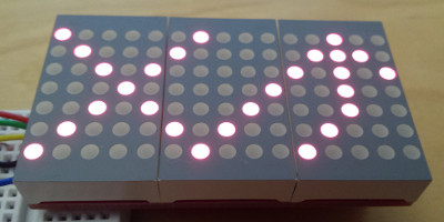
LED matrix tile
24 November 2018The 2nd generation LED matrix display was from the outset a prototype for a circuit that can be tiled, and this article covers the follow-on tile itself. The idea is that the entire PCB is under the envelope of the LED chips, so that they can be tiled horizontally or vertically into a larger display. I had intended to leave LED matrix projects alone until I had written some software to aid the creation of display data, but Seeedstudio had a special offer on, and I could not think of an alternative project in the short time available.
Circuit design choices
The circuit is more or less that of the stripboard-based 2nd generation display redesigned to use fewer components: The set of PNP transistors together with the associated base resisitors have been replaced with a single Darlington array chip, and instead of multiplexing with D-type latches all the LED columns are directly connected to the micro-controller. All the circuitry was required to fit on the underside of the PCB, between the pins for the LED matrix chips, as shown below:
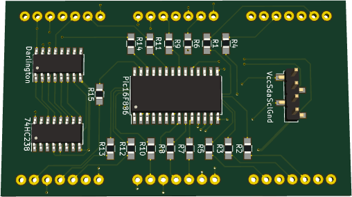
Because the top side is entirely covered by the LED chips, all components on the under-side had to be surface-mount, most notably the external interface pins. For all the chips I opted for SOIC packages, because they are that bit easier to hand-solder compared to SSOP/TSSOP due to the relative ease of avoiding solder bridges. Below are some remarks regarding specific components and design choices.
LED matrix chips
Rather than using LED matrix modules, the LED chips are soldered directly onto the PCB, and unlike the previous circuits row-cathode chips are used instead of column-cathode — see later discussion on stock issues for order numbers. The latter change was done purely to accomodate the Darlington array chip, as descibed in the next section. Although the circuitry could have fitted under two LED chips, the 15 columns of three chips is a better fit to the 16 bits in two bytes.Darlington array
I had looked for a PNP array chip that could have been a direct replacement of the discrete transistors but could not find a suitable one, so I opted for a Darlington array chip that is in effect an array of NPN transistors. The chip is a Texas InstrumentsSN75468D (Farnell 9593004) which with only one collector conducting at once can sink 350mA, which at 23mA per column is vastly in excess of what all the other components can sustain.
Main controller
This circuit is my first use of thePIC16F886 microcontroller, which was chosen purely due to the large number of I/O pins it has in a SOIC package. Two whole ports are dedicated to just the columns and the lowest three bits of a third port controls the 74HC238, which avoids the need for mapping within the firmware. While it is not part of PIC12F18xx/PIC16F182x family of PIC microcontrollers I was aiming to consolidate on, the largest chip in that family had fewer I/O pins. However the only special feature this circuit uses is I2C, which is much the same on all PIC microcontrollers.
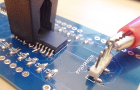
In-circuit programming
For this circuit I decided to forego having a programming header, due to the space requirement of my usual 6-pin 2.54mm receptacle, and instead use a test clip that attaches to the microcontroller itself when it is mounted on the PCB, as shown below. However a 20-pin clip is needed to make contact with all the programming and power pins, and the largest test clip I was able to source at reasonable cost was only 16 pins. Since the two Ground pins are connected together on the PCB the only unconnected pin is Vcc, and for this one pins I decided easiest thing to do was to connect a fly-lead to the Vcc pin of the external interface, as shown below:
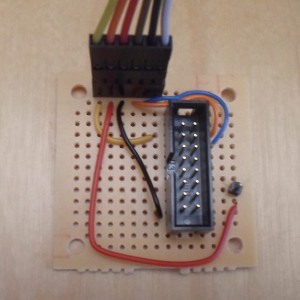
I had thought of other solutions such as using two smaller test clips, and using a 4-wire IDC cable (e.g. Samtec IDSS-04-D-05.00 — Farnell 2598236) rather than a crocodile fly-lead, but in the end I decided to use what I had at hand that was suitable for the task. The smaller test clips were intended for narrower SOIC chips, and I felt that the Samtek lead was a bit on the pricey side. Anyway I soldered up a some perfboard to act as an adapter for the connection with PicKit, after doing a quick test with a make-shift adapter wired up on solderless breadboard, and the former is shown below.
Doing away with an explicit programming interface was really out of necessity with the PCB, due to lack of space and the clearance required for an external connector, but it was nevertheless the first time I used the approach of a clip to go over the chip itself. I like SOIC chips as they are smaller than DIP, which don't have any real advantage on PCBs when being soldered directly rather than via a socket, but are easier to solder than SSOP/TSSOP due to having a lot less tendency to get solder bridges. Using the chip itself as the flash connector is convenient in these circumstances.
LED current rating
Each I/O pin on thePIC16F886 can source 25mA, although the real limitation is the maximum 95mA that the chip can draw through its power pins, which works out at a bit above 6mA per column. When doing brightness tests with the previous display circuit I thought 500Ω would give acceptable brightness and would draw a touch below 6mA, although I ultimately went for 510Ω resistors because 500Ω 0805 (2012 metric) ones were several euro each whereas the former were €4 for 1000. I did not intend to do power measurements with this circuit, but for reasons unrelated to LED brightness I ended up taking readings anyway, and these are shown below — inside and outside refer whether the measurements were taken “inside” the circuit between the voltage regulator and the PCB, or on the external side of regulator. Prototype refers to the previous second-generation circuit and this value is “outside”.
| Remark | Dots lit (mA) | ||
| 5 | One row | All rows | |
| Prototype | 12.66 | ||
| PCB outside | 12.41 | 33.33 | 54.5 |
| PCB inside | 8.95 | 28.6 | 48.83 |
These measurements were made with a 12volt mains-supplied DC power supply connected to the voltage regulators, so lack of power is not an issue. The fuse in my multimeter blew so I did not get all the readings for the second-generation board, but of the reading I did get I can conclude its power consumption is not significantly different, with the higher LED protective resistances being offset by lower LED matrix chip voltage drops. The ~49mA draw from having all LEDs lit comes out at 3.3mA per dot/column, which is about half what I expected.
Power supply resilience
One thing I noticed with this circuit compared to the second-generation circuit was resilience to marginal power supply. The second-generation circuit still operated as expected when the voltage across the power supply regulator was only 4.5volts, whereas using the same 9-volt power cell was unable to power the LED tile PCB enough for proper operation. This observation is why I performed current-draw measurements above, in part because I had not realised how depleted the power cell I used was, but these measurements indicated that with an unstrained power supply actual power consumption was about the same with both circuits.
The resilience to marginal voltages is most likely because the current draw from the microcontroller in the second-generation circuit is basically nothing — column control is via D-Type latches that have high-impedance inputs, and row-control is via a decoder chip that in turn just activates power-supply transistors. In contrast the PIC16F886 is the current source for the LED matrix chips, and the peak power demands are a good proportion of the chip's specified maximums, so the power drops on the output pins cause improper operation.
The firmware
The firmware for the circuit — which is in Bitbucket and based on the previously-unpublished firmware used for the second-generation circuit — has few things worth mentioning that were not covered previously. Most of the required changes were due to hardware differences, such as different pin-outs and configuration register bits. For some reason PIC microcontrollers are inconsistent in the naming of I2C-related registers — for instanceSSP1CON1 on the PIC16F1828 versus SSPCON on the PIC16F886 — even though the bit-fields within them are all the same. However some other changes were made for efficiency reasons, and this is the general subject of the next sub-sections. A major theme is C code versus writing routines in PIC assembly.
Clock speed & LED pulse time
Back this time last year when I was building the original LED matrix display I worked out that in order to avoid flicker, the total refresh time needs to be 25ms or less. With the latest circuit the refresh time is mostly a function of the LED pulse-time, which is linked to clock speed FOsc and the Timer2 post-scale ratio (pre-scale is set to 1:1 andPR2 to 255), for which pre-calculated values are shown in the table below. I am unsure if these calculations are accurate, but I do know from experimentation that parameters with a notional refresh time above 25ms show flickering, whereas ones below do not. The “ideal” parameter set for exactly 25ms is shown in bold for reference.
| FOsc | Postscale | Refresh time |
| 500kHz | 1:1 | 14.3ms |
| 2MHz | 1:5 | 17.9ms |
| 1MHz | 1:3 | 21.5ms |
| 4MHz | 1:13 | 23.3ms |
| ~2MHz | 1:7 | 25ms |
| 2MHz | 1:7 | 25.1ms |
| 1MHz | 1:4 | 28.7ms |
| 500kHz | 1:2 | 28.7ms |
| 1MHz | 1:5 | 35.8ms |
Main thing of interest is that it is possible to use a relatively low clock speed of 500kHz, and still have a sufficiently fast total refresh time. Technically the circuit could do away with any controlled pulse time and simply cycle though all seven rows as quickly as possible, but I think it better not to leave duty cycles down to unpredictable code execution time.
Array looping efficiency
In PIC code looping over an array using a variable is notably inefficient, as the resulting assembly introduces a lot of code into each iteration which seem to be related to bank switching and carry bits. For instance consider the functionledClear(), for which two implementations are in the code snippet below: One using a loop and one that is manually unrolled using hard-coded values:
void ledClear(void) { #ifndef UNROLL_LOOP unsigned char idxRow; for(idxRow=0; idxRow<7; idxRow++) ledCol1[idxRow] = 0; #else ledCol1[0] = 0; ledCol1[1] = 0; ledCol1[2] = 0; ledCol1[3] = 0; ledCol1[4] = 0; ledCol1[5] = 0; ledCol1[6] = 0; #endif }
The first (UNROLL_LOOP not defined) results in a loop iteration — shown below — that consists of 24 instructions and makes use of three temporary registers. r0x102D is idxRow, and my best guess is that the other two are for the calculation of the indirection address.
_ledClear: BANKSEL r0x102D CLRF r0x102D _00130_DS_: BANKSEL r0x102D MOVF r0x102D,W ADDLW (_ledCol1 + 0) MOVWF r0x102E MOVLW high (_ledCol1 + 0) BTFSC STATUS,0 ADDLW 0x01 MOVWF r0x102F MOVF r0x102E,W BANKSEL FSR MOVWF FSR BCF STATUS,7 BANKSEL r0x102F BTFSC r0x102F,0 BSF STATUS,7 MOVLW 0x00 BANKSEL INDF MOVWF INDF BANKSEL r0x102D INCF r0x102D,F MOVLW 0x07 SUBWF r0x102D,W BTFSS STATUS,0 GOTO _00130_DS_ RETURN
In contrast the hard-coded manual loop unrolling (UNROLL_LOOP is defined) results in the assembly output shown below, which in total is nine instructions — less than half of just one iteration in the code above. I'm not sure if all the instructions above are strictly necessary, but in terms of run-time the loop will always be significantly worse. The PIC assembly set is very much biased towards things being hard-coded, and a much more aggressive optimising C compiler would probably output the code below in response to an array-clearing loop.
_ledClear: BANKSEL _ledCol1 CLRF (_ledCol1 + 0) CLRF (_ledCol1 + 1) CLRF (_ledCol1 + 2) CLRF (_ledCol1 + 3) CLRF (_ledCol1 + 4) CLRF (_ledCol1 + 5) CLRF (_ledCol1 + 6) RETURN
As an aside, and I have remarked on this in the past, is the style of programming that comes with embedded code such as this firmware — a programming style that from the perspective of desktop programming is outright bad. Cut'n'pasted code with hard-coded constants has almost pariah status with desktop programming, but with embedded firmware it is a practical necessity due to the relative stateless nature of the systems, which is reflected by the balance between available RAM and program flash space: On the PIC16F866 368 bytes versus 8192 words, with 368 bytes being an unusually large amount for a PIC microcontroller.
Rewriting the data-flip routines
A problem that occurred as a result of a low clock speed of 500kHz is a noticeable blink when the display is updated via I2C. The quick solution was to use a much higher clock speed, but the underlying problem is the computationally-expensive nature of the data-flip done when updated display data is received. This data flip takes the column data that is received via I2C and converts it into row-orientated data that is better suited to how the circuit does the refresh cycle. Doing this with byte-orientated memory access results in a somewhat tricky algorithm, which in turn compiles to a lot of instructions for reasons already covered. Flipping is much better suited to bit-orientated addressing, which unfortunately means hard-coding the lookup of each bit within the column data and the subsequent write to the row data. The handling of a single column is shown in the assembly snippet below:ledCol1[7] = bufCols[0]; __asm BANKSEL _ledCol1 BTFSC (_ledCol1 + 7),0 BSF (_ledCol1 + 0),0 BTFSC (_ledCol1 + 7),1 BSF (_ledCol1 + 1),0 BTFSC (_ledCol1 + 7),2 BSF (_ledCol1 + 2),0 BTFSC (_ledCol1 + 7),3 BSF (_ledCol1 + 3),0 BTFSC (_ledCol1 + 7),4 BSF (_ledCol1 + 4),0 BTFSC (_ledCol1 + 7),5 BSF (_ledCol1 + 5),0 BTFSC (_ledCol1 + 7),6 BSF (_ledCol1 + 6),0 __endasm;
The major trick here is copying the column data into the same array as the row data, which seems to be the only way to guarantee that the source columns and destination column data storage is in the same bank. This avoids having loads of bank selection instructions — without which data-corruption is inevitable — which is critical because the bit-checking conditional branch is a fixed single instruction jump, and PIC assembly does not have a relative jump. With an overhead of eight instructions for an initial clear and six instructions per column for the copy-in, this is two instructions per display dot, which works out a total of 308 instructions executed to do the data-flip. In contrast within the byte-orientated C code the while loop for columns compiles to 101 instructions, of which 68 are an internal for-loop — a quick calculation is the whole lot needing 7,635 instruction executions, about 25 times what the hard-coded assembly requires. At a clock speed of 500kHz this is 1.2ms versus 30.5ms.
LED matrix availability
Farnell regards the Multicomp LED matrix chips as a legacy product, and back in July I noted the stock levels of them, with a punt that the remaining stocks would last about a year or so. The updated stock levels at time of writing are given below:
| Multicomp code | Colour | Polarity | Farnell code | Farnell stock |
703-0192 |
Green | Row cathode | Gone | |
703-0193 |
Green | Column cathode | 2112219 | 627 |
703-0194 |
Red | Row cathode | 2112221 | 63 |
703-0195 |
Red | Column cathode | Gone | |
Aside from the green column-cathode 703-0193 units which have hardly sold at all in the preceding three months, the remaining units have gone quickly, and when I bought some of the red row-cathode 703-0194 in the latter part of last September ago I worked on the basis that it would probably be my last chance to stock up on them. I did consider clearing the shelf of all then-remaining 113 units, but in the end settled for buying 50 units — enough to fill out all ten tile PCBs I had ordered, plus a few more. My July prediction of the remaining stock lasting a year is probably accurate, but the range has shrunk quicker than I expected — for the remaining red chips, I would suggest securing stock before designing any circuits, but the green chips should last.