NXP NT3H2211 NFC tag
14 November 2017The NXP
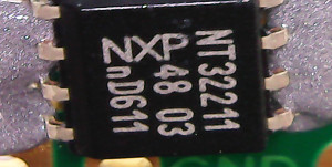
NT3H2211-W0FT1 (data-sheet) is an RFID chip I bought off Digi-Key (stock code 568-12905-1-ND) back in June before I really knew what I was doing, and finally got round to mounting it on a breakout board — although the chip itself was quite cheap, the shipping costs were somewhat steep, so getting round to soldering the chip to the breakout board was something I kept on putting off. Since this is the first SMD integrated circuit I have reflow soldered, I have documented the experience.
For testing purposes I got as far as attaching an NFC antenna, writing an NFC record to the chip via I2C, and then reading the message using an NFC reader. This article only covers the NFC message specification to the extent needed to construct the test message, as the NFC message format is not really an electronics issue. As a result I also make no guarantees on the correct use of NFC terminology.
Mounting the chip
I was going to try surface mounting the chip using a soldering iron, and had got in a bottle of flux (Edsyn FL911, Farnell 2576913), but in the end decided to hot-plate reflow this chip as well. After buying in a few different breakout boards, I settled for the Roth RE899 breakout board (Farnell 2474677), due to it being the correct size and since it came without pins attached I could hot-plate reflow it like I did with SMD resistor array & Sziklai transistor pair boards.Adding paste
For this chip I simply put a strip of solder paste across all the pins and then placed the chip on top, which is the common technique in the absence of a solder stencil mask. As can be seen below this is clearly excess, but this in itself is not a major problem. I concluded that removing solder bridges would be easier than trying to put down the exact amount of paste required.
Fixing solder bridges
Quite predictably given the amount of solder paste used, I got solder bridges that needed removal after the reflow was complete. I am told the technique for getting rid of solder bridges is to put down flux and then pull away the excess solder with a soldering iron, but I ended up having to use some de-soldering ribbon (Farnell 252505) as well. Below shows the results before and after — I took off the chip labelling in the process, which makes me wonder whether I used the correct technique, but it did not seem to affect the operation of the chip.
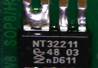
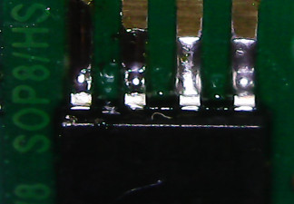
The bottom half actually had bridges across all the pins, so having only one bridge on the top half as shown is actually a bit of a surprise. Just as well I took a picture of the bridges, as without the label that got removed in the process, it is hard to tell what the orientation of the chip is.
Smoke-testing the chip
Although I was not originally planning on using the mounted chip for some time, I decided to give it a quick test, just to make sure it was in at least some form of operational order and not completely burned out. The test itself was simple — see if any internal state can be read over the I2C interface. If this was successful it would indicate the chip is not bricked, and that at least four of the pin connections are in a good state.
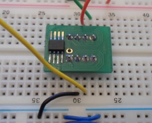
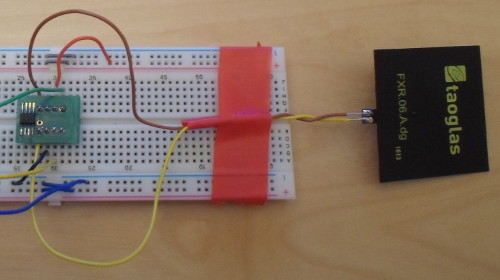
For the test I put the breakout board onto solderless breadboard and wired it to my I2C-USB master, as shown above. I then used my Python serial Tx/Rx script ttyTxRx.py for the test, as shown in the console dump below. The first command sets up the I2C-USB master. The second initiates a 16 byte read from internal address 0x00 on the chip, which itself uses I2C address 0xab.
$ ./ttyTxRx.py /dev/ttyACM0 1 5a 02 60 04 Sending 4 bytes.. Sent 4 Replies (1 expected): 0xff $ ./ttyTxRx.py /dev/ttyACM0 16 55 ab 0 16 Sending 4 bytes.. Sent 4 Replies (16 expected): 0x4 0x21 0x4e 0xa 0x7 0x4f 0x80 0x0 0x44 0x0 0x0 0x0 0x0 0x0 0x0 0x0
The first seven bytes is the device serial number, of which the first is always 0x04. This was enough to convince me that I had an operational chip, even though at the time I had yet to attach an antenna.
Attaching an antenna
For a more sophisticated test, namely testing actual functionality of the chip, I needed to attach an antenna. Although I originally stocked a small cross-section of antennas when I bought in the chip, the one I ended up using is a TaoglasFXR.06.A.DG (Digi-key 931-1418-ND), to which I needed to solder fly-leads. The fully-assembled setup, even though there is not much to it, is shown below:
Coming in at €8 I think the Taoglas antenna is grossly over-priced, but it got the job done. I have yet to get around to seeing how some of the cheaper antenna perform — such as 553-2633-ND which is only €1.38 and I am sure there are cheaper ones out there — but for this circuit where the chip has an external power supply I suspect any 13.56MHz antenna will do.
Setting up the chip
To test the functionality of the chip itself, namely reading & writing of NFC data, requires quite a bit of up-front work. Much of the information here I mined from the NFC Type 2 Tag spec (v1.1), but without reading it from end-to-end it is not the clearest of documentation. I specifically avoided downloads that required agreeing to a licence, but I suspect the documents on the NFC consortium website are probably not significantly clearer. I was only after a minimal setup, so options like write-protect & security are beyond the scope of this article.Setting the CC
The Capability Container is a 4-byte word that gives basic information about an NFC device's data area, and this has to be set before theNT3H2211 can be useful for anything. It gives basic information about the data contained in the chip's user memory, and the chip's data-sheet gives example values for these Capability Container bytes. These bytes break down as follows:
- Magic number
0xe1 - A fixed value. Indicates NDEF data present.
- Version number
0x10 - Corresponds to v1.0 of the Type 2 Tag Platform — I suspect it two nibbles of 4 bytes each.
- Data area size
0x6d - This value is multiplied by eight, so in this case covers all 868 bytes of the first bloc of user data. Unlike the
NT3H2111theNT3H2211has a second data block, but I did not make use of the extra capacity. - Security flags
0x00 - No restrictions on reading or writing.
NT3H2211 is that it only supports reads/writes via I2C in 16-byte blocks, and since the Capability Container bytes are at the end of the first block, this leads to loads of pit-falls:
- Although reading byte zero always gives
0x04, writing to it changes the chip's I2C device address. - The next 6 bytes are the device-unique part of the device serial number, which are actually write-protected.
- The 5 bytes after that are listed in the data-sheet as internal so purpose is not known.
$ ./ttyTxRx.py /dev/ttyACM0 1 55 aa 0 10 ab 21 4e a 7 4f 80 0 44 0 0 0 e1 10 6d 0 Sending 20 bytes.. Sent 20 Replies (1 expected): 0x1
The data is persistent, so it will not be reset to zeros if the device is powered down. Even though writing less than 16 bytes is reportedly successful, doing so will not actually result in the bytes being written.
Writing NDEF Messages
What caught me out is that the data area is more than just a bunch of NDEF records — an NDEF Message (i.e. a collection of NDEF Records) has to be contained within a TLV, so the content of the data area is as follows:- NDEF Message TLV:
0x03 0x12 - Container for NDEF Messages. The 2nd byte is length, and if its value is
0xffthe length is actually encoded in a further two bytes. - NDEF Record
- An NDEF URI record, which is detailed below.
- NDEF Terminator TLV:
0xfe - Indicates no more data in the memory area. Suspect it stops the reader from reading further bytes.
- NDEF NULL TLV:
0x00 - Padding bytes.
NDEF Message Record
A full break-down of the NDEF Message format is beyond the scope of this article, so only the basics are covered here for a single self-contained message. Each NDEF Message is a collection of NDEF Records, the latter of which is detailed below. The first byte is a header that contains mainly bit-fields, whereas the rest of the Record is byte-orientated.
| Bit 7 | Bit 6 | Bit 5 | Bit 4 | Bit 3 | Bits 0-2 | ||
| First Record | Last Record | Chunked | Short Record | ID field present | Type Name Format | ||
- First Record
- Flag is set since this is a single-record message.
- Last Record
- Flag is also set since this is a single-record message.
- Chunked
- Chunked message. I have not looked into the details, but suspect it much like HTTP Chunking.
- Short Record
- Payload length field is a single byte rather than four bytes.
- ID Field
- Not set, so the ID Field & ID Field Length are absent.
- Type Name Format
- Indicates record type. The value
0x01is “well-known record”, which is basically an NFC built-in message type that is compact.
- Header:
0xd1 - A standalone self-contained NDEF Record. Header details are above.
- Type field size:
0x01 - The size of the type field.
- ID field length: absent
- Length of the ID field below. Not present as the ID Field bit in the header is not set.
- Payload length:
0x0e - Length of payload, which is 14 bytes. Since the Short-Record bit is set in the header, this is a single byte rather than a 4-byte word.
- Type field:
0x55 - ASCII code for 'U', which indicates a URI record.
- ID field: absent
- Not used.
- Payload:
0x03 0x6d 0x2e 0x72 0x65 0x6d 0x79 0x2e 0x6f 0x72 0x67 0x2e 0x75 0x6b - The first byte
0x03indicate that the URI is to be pre-pended with thehttp://prefix. The remaining bytes are the URI itself.
The complete setup messages
The whole message test-data spans two 16-byte blocks, so they each need to be written using separate commands. These commands are shown below, making use of thettyRxTx.py script. The second command needs the padding out with zeros.
$ ./ttyTxRx.py /dev/ttyACM0 1 55 aa 1 10 3 12 d1 1 e 55 3 6d 2e 72 65 6d 79 2e 6f 72 Sending 20 bytes.. Sent 20 Replies (1 expected): 0x1 $ ./ttyTxRx.py /dev/ttyACM0 1 55 aa 2 10 67 2e 75 6b fe 0 0 0 0 0 0 0 0 0 0 0 Sending 20 bytes.. Sent 20 Replies (1 expected): 0x1
Reader test
To test the programmed chip I used an NXPOM5577, which is a development board for the RaspberryPi that contains a PN7120S (data-sheet) NFC read/write chip. I used the RaspberryPi Linux image supplied by NXP, which includes a sample program used to read the NT3H2211. The output of a successful read is shown below:
Waiting for a Tag/Device... NFC Tag Found Type : 'Type A - Mifare Ul' NFCID1 : '04 21 4E 0A 07 4F 80 ' Record Found : NDEF Content Max size : '868 bytes' NDEF Actual Content size : '18 bytes' ReadOnly : 'FALSE' Type : 'URI' URI : 'http://m.remy.org.uk' 18 bytes of NDEF data received : D1 01 0E 55 03 6D 2E 72 65 6D 79 2E 6F 72 67 2E 75 6B NFC Tag Lost
Personally I would prefer to build my own image based on Slackware rather than use the probably-dated reference image provided by NXP, but for testing purposes this is a moot point. I probably would have used a USB reader/writer for testing if I had one at hand.Remarks
I had originally just intended to remark on the reflow soldering of the chip, since it is the first integrated circuit I have reflowed, but for testing I ended up going as far as writing data to the chip. The chip itself seems somewhat agnostic about the data within the user memory area, so things like NDEF Message structure is not really an electronics issue — it is protocol work. Interest in this chip was always as a potential building block in a larger project, but I never got round to starting such. I suspect it was latent memories of a project my brother suggested, but at the time did not have the resources (time mainly) to investigate properly.I did have a look at some of the access control features, but they seem to only affect the NFC interface rather than the I2C one, and it all amounts to just more reading/writing. With NFC the real sophistication is in the reader/writer rather than the tag, so I doubt there is much else to learn about the chip without diving into the complexities on the other side. This would involve either the RaspberryPi I used for testing, or a USB-based reader/writer, and in either case would not really be an electronics project. Looking into all this protocol stuff is really a software project, although I suspect I will do so at some point in the future.