NXP LPC1112 Cortex-M0 I/O
28 December 2018A while ago I obtained some ARM Cortex-M0 chips and got both a development setup and a very basic firmware working, but since then had on my to-do list finding out how to get various input/output sub-systems working so that the chip would be of practical use: simple pin read/writes, RS232 communications, and I2C interfacing. This article covers these topics, complete with references to sample ARM code within my Bitbucket repository — my focus is on minimalist from-scratch samples so there are no dependencies beyond the hardware and tool-chain.
While my first Cortex-M0 firmware was functional, there were faults that only became apparent when writing more sophisticated firmware, such as not zeroing out memory within the .bss code segment. I also wanted to seperate the boiler-plate interrupt handlers into a chip-specific stub, leaving a simplified API for me to build firmware programs on top of — I have no doubts that I will end up extending this stub to allow for more functonality. A notable change in the process was rigging the linker script so that the checksum value that the LPC1112 expects is not affected by code outside of the stub.
Building a more recent ARM GCC
Unlike the other Slackware tool-chain components the SlackBuild for ARM GCC uses GCC v4.9.2 which is rather dated, but it is pretty easy to use the same script to build the more recent v7.4.0 instead — the relevant commands are listed below. The patch gcc7arm.patch changesVERSION=${VERSION:-4.9.2} to VERSION=${VERSION:-7.4.0} so that the script uses the correct version number, and gcc-$VERSION.tar.bz2 is changed to gcc-$VERSION.tar.gz since GCC no longer ships in BZip2 archives.
wget https://slackbuilds.org/slackbuilds/14.2/development/arm-gcc.tar.gz tar -xzvf arm-gcc.tar.gz patch -p0 < gcc7arm.patch cd arm-gcc wget ftp://ftp.gnu.org/pub/gnu/gcc/gcc-7.4.0/gcc-7.4.0.tar.gz ./arm-gcc.SlackBuild installpkg /tmp/arm-gcc-7.4.0-x86_64-1_SBo.tgz
Note that the last two commands have to be run as root. See my previous article for other tool-chain details
Basic pin configuration
Within theLPC111x user manual the section that covers pin configuration is 37 pages long, and this section distills down the information relevant to the pins that appear on the 20-pin LPC1112. Although each pin is configured using a 32-bit register only the bottom eleven are used, and the purpose of each bit is summarised in the table below with defaults highlighted in bold. The I2C-capable pins (5 and 20) have an on-reset default of 0x00 whereas all the other pins have a reset value of 0xd0. Note that for ports not capable of analogue input bit 7 has no effect, but the chipset specs adopt the convention of having it default to set (i.e. high) for digital-only ports anyway. For some reason Bit 6 also defaults to high even though no pin uses it.
| Bits | ||||||||||||
| 0 | 1 | 2 | 3 | 4 | 5 | 6 | 7 | 8 | 9 | 10 | 11-31 | |
| Pins 1-3 Pins 5-6 Pins 11-12 Pins 17-20 |
Function | Mode | Hysteresis | reserved | Analog/Digital | reserved | Output | reserved | ||||
| See Pin Functions |
0x0 Inactive 0x1 Pull-down 0x2 Pull-up 0x3 Repeater mode |
0x0 Off 0x1 On |
0x0 Analog 0x1 Digital |
0x0 Normal GPIO 0x1 Pseudo-drain |
||||||||
| Pin 4 Pins 7-10 |
reserved | |||||||||||
| Pin 5 Pin 20 |
Function | reserved | I2C Mode | reserved | ||||||||
| 0x0 GPIO 0x1 I2C |
0x0 Standard/Fast I2C 0x1 Standard I/O 0x2 Fast+ I2C |
|||||||||||
Configuration notes
- Mode
- Mode is whether internal pull-up and pull-down resistors are enabled. When mode is inactive it means input is neither pulled up nor pulled down, and repeater mode uses feedback so that if the input becomes floating the input port retains the previous driven value. Mode should be zero for analog input.
- Hysteresis
- When enabled hysteresis uses different voltage thresholds for low-to-high and high-to-low transitions, which is meant to avoid toggling in the presence of line noise. I suspect it is implemented using a Schmitt trigger. Hysteresis must be disabled when the power supply is less than under 2.5 volts.
- Output
- Pseudo-drain output mode is where the pin is either pulled to zero or left floating. It is implemented using a strong pull-down rather than a transistor open-drain.
- I2C pins
- The I2C-capable pins are a bit different in that when they are configured as GPIO, they are open-drain rather than driven via strong pull-up & pull-down. Standard/Fast I2C includes a glitch filter and is intended for I2C clock speeds upto 400kHz, whereas Fast+ I2C uses a high-current sink for clock speeds of 400kHz-1MHz. Fast+ I2C should not be selected when pin is being used for GPIO. The purpose of Standard I/O is not made clear in the chipset documentation.
Pin functions
The functions available on each pin are shown in the table below, which is sorted by ascending configuration register address rather than pin number. Although the configuration registers allow a pin to have seven different functions, all pins only have between two and four different functions, and in all cases GPIO is either0x0 or 0x1.
| Address | Pin | GPIO Port | Function 0x00 (default) | Function 0x01 | Function 0x02 | Function 0x03 |
0x4004400c |
17 | Port 0 Bit 0 | Reset (active low) | GPIO | reserved | |
0x40044010 |
18 | Port 0 Bit 1 | GPIO | ClkOut | CT32B0_MAT2 | reserved |
0x4004401c |
19 | Port 0 Bit 2 | SSEL0 | CT16B0_CAP0 | ||
0x40044030 |
20 | Port 0 Bit 4 | GPIO (open drain) | I2C SCL | reserved | |
0x40044034 |
5 | Port 0 Bit 5 | I2C SDA | |||
0x4004404c |
6 | Port 0 Bit 6 | GPIO | reserved | SCK0 | reserved |
0x40044060 |
1 | Port 0 Bit 8 | MISO0 | CT16B0_MAT0 | ||
0x40044064 |
2 | Port 0 Bit 9 | MOSI0 | CT16B0_MAT1 | ||
0x40044068 |
3 | Port 0 Bit 10 | SWCLK (debugger clock) | GPIO | SCK0 | CT16B0_MAT2 |
0x40044074 |
4 | Port 0 Bit 11 | reserved | Analog input | CT32B0_MAT3 | |
0x40044078 |
7 | Port 1 Bit 0 | CT32B1_CAP0 | |||
0x4004407c |
8 | Port 1 Bit 1 | CT32B1_MAT0 | |||
0x40044080 |
9 | Port 1 Bit 2 | CT32B1_MAT1 | |||
0x40044090 |
10 | Port 1 Bit 3 | SWDIO (debugger I/O) | CB32B1_MAT2 | ||
0x400440a4 |
11 | Port 1 Bit 6 | GPIO | RXD | CT32B0_MAT0 | reserved |
0x400440a8 |
12 | Port 1 Bit 7 | TXD | CT32B0_MAT1 | ||
| n/a | 13 | n/a | XTALIN (input to internal clocking circuits) | |||
| 14 | XTALOUT (oscillator amplifier out) | |||||
| 15 | Vcc power connection | |||||
| 16 | Ground power connection | |||||
General Purpose Input/Output
My natural inclination would be to leave low-level bit-banging to PIC Microcontrollers and use ARM for higher-level processing, but since GPIO is the most basic way to test that a chip is actually working, configuring pins for this functionality is presented here. Since there is not that much to GPIO anyway — the relevant chapter within the user guide is only eight pages long — I decided to make this section complete as well. GPIO-specific functionality is accessed through the registers shown in the table below — with all GPIO registers the bottom twelve bits (i.e. bits 0 thru 11 inclusive) correspond to the pins within a GPIO port, although on theLPC1112 not all of these pins will be used.
| Address | Description | |||
| Port 0 | Port 1 | Name | Effect when Low | Effect when High |
0x50003ffc |
0x50013ffc |
Data read/write | See GPIO reads & writes | |
0x50008000 |
0x50018000 |
Direction | Input pin | Output pin |
0x50008004 |
0x50018004 |
Interrupt Sense | Edge trigger | Level trigger |
0x50008008 |
0x50018008 |
Interrupt Both Edges | See Interrupt Event | Both edges trigger |
0x5000800c |
0x5001800c |
Interrupt Event | Trigger on falling/low | Trigger on rising/high |
0x50008010 |
0x50018010 |
Interrupt Mask | Interrupt masked out | Interrupt enabled |
0x50008014 |
0x50018014 |
Raw Interrupt State | No interrupt | Interrupt occurred |
0x50008018 |
0x50018018 |
Masked Interrupt State | No (or masked out) interrupt | Interrupt occurred |
0x5000801c |
0x5001801c |
Interrupt Clear | No effect | Clear edge detection |
By default GPIO pins are input with built-in pull-up enabled. I am not sure if setting the corresponding bits of both interrupt sense and interrupt both edges is valid. Note that if a floating pin is switched from output to input the value it returns upon a subsequent read will be unpredictable. Ports 2 and 3 would use addresses in the ranges 0x5002xxxx and 0x5003xxxx respectively if they were present
GPIO interrupts
I have tended to prefer polling rather than interrupts when writing control firmware, but GPIO shows quite nicely how interrupts operate on theLPC1112. Edge-triggered interrupts remain asserted until reset using the 0x500x801c register, whereas level-sensitive interrupts remain asserted until the level changes away from the trigger level. A consequence of the latter is that the interrupt handler will be continually called unless the pin is masked out. The difference between the raw and masked interrupts is that only interrupts that are not masked out will cause the interrupt handler to be called. My LPC1112 GPIO demo uses edge-triggered interrupts to implement an LED toggle.
GPIO reads and writes
For a read or write the lower bits of the address are a bit-mask — for a read the returned value will be the logical-and of the pin states and this bit-mask, and for a write the set bits within the bit-mask indicate which pins will be set rather than left unchanged. There is a gotcha though, and that is the bit-mask occupies bits 2 thru 13 rather than the bottom twelve bits, so the bit-mask is effectively shifted up two bits — this is because addresses in ARM code have to be a multiple of four, so the bottom two bits cannot form part of the mask. Some of the mappings between address and bits affected are shown in the table below:
| Address | Bits affected | ||||||||||||
| Port 0 | Port 1 | 0 | 1 | 2 | 3 | 4 | 5 | 6 | 7 | 8 | 9 | 10 | 11 |
0x50000000 |
0x50010000 |
✘ | ✘ | ✘ | ✘ | ✘ | ✘ | ✘ | ✘ | ✘ | ✘ | ✘ | ✘ |
0x50000004 |
0x50010004 |
✔ | ✘ | ✘ | ✘ | ✘ | ✘ | ✘ | ✘ | ✘ | ✘ | ✘ | ✘ |
0x50000008 |
0x50010008 |
✘ | ✔ | ✘ | ✘ | ✘ | ✘ | ✘ | ✘ | ✘ | ✘ | ✘ | ✘ |
0x50000010 |
0x50010010 |
✘ | ✘ | ✔ | ✘ | ✘ | ✘ | ✘ | ✘ | ✘ | ✘ | ✘ | ✘ |
0x50000020 |
0x50010020 |
✘ | ✘ | ✘ | ✔ | ✘ | ✘ | ✘ | ✘ | ✘ | ✘ | ✘ | ✘ |
0x50000040 |
0x50010040 |
✘ | ✘ | ✘ | ✘ | ✔ | ✘ | ✘ | ✘ | ✘ | ✘ | ✘ | ✘ |
0x50000080 |
0x50010080 |
✘ | ✘ | ✘ | ✘ | ✘ | ✔ | ✘ | ✘ | ✘ | ✘ | ✘ | ✘ |
0x50000100 |
0x50010100 |
✘ | ✘ | ✘ | ✘ | ✘ | ✘ | ✔ | ✘ | ✘ | ✘ | ✘ | ✘ |
0x50000200 |
0x50010200 |
✘ | ✘ | ✘ | ✘ | ✘ | ✘ | ✘ | ✔ | ✘ | ✘ | ✘ | ✘ |
0x50000400 |
0x50010400 |
✘ | ✘ | ✘ | ✘ | ✘ | ✘ | ✘ | ✘ | ✔ | ✘ | ✘ | ✘ |
0x50000800 |
0x50010800 |
✘ | ✘ | ✘ | ✘ | ✘ | ✘ | ✘ | ✘ | ✘ | ✔ | ✘ | ✘ |
0x50001000 |
0x50011000 |
✘ | ✘ | ✘ | ✘ | ✘ | ✘ | ✘ | ✘ | ✘ | ✘ | ✔ | ✘ |
0x50002000 |
0x50012000 |
✘ | ✘ | ✘ | ✘ | ✘ | ✘ | ✘ | ✘ | ✘ | ✘ | ✘ | ✔ |
0x50003ddc |
- | ✔ | ✔ | ✔ | ✘ | ✔ | ✔ | ✔ | ✘ | ✔ | ✔ | ✔ | ✔ |
| - | 0x5001033c |
✔ | ✔ | ✔ | ✔ | ✘ | ✘ | ✔ | ✔ | ✘ | ✘ | ✘ | ✘ |
0x50003ffc |
0x50013ffc |
✔ | ✔ | ✔ | ✔ | ✔ | ✔ | ✔ | ✔ | ✔ | ✔ | ✔ | ✔ |
The address nibbles 0x3ddc and 0x033c mask out the pins that are not physically present on ports 0 and 1 respectively. Reading of a pin that is not setup as a GPIO still returns the pin’s actual state, which may well be random — hence why it is worth masking out non-GPIO inputs during reads.
Attaching a debugger
The GPIO demo is a good choice for showing the attachment of a debugger, and a simple debugging session is presented below to show the basic commands — highlighed in bold — that are specific to debugging firmware rather than desktop applications. The OpenOCD documentation covers using GDB, so consult the latter for details. One major pit-fall is that Windows GDB does not properly handle Ctrl-C, so you may want to use a Linux box for firmware development — at time of writing I was overseas and hence relegated to using a Windows10 laptop.$ arm-none-eabi-gdb gpio.elf Output omitted (gdb) target remote localhost:3333 Remote debugging using localhost:3333 ARMmain () at gpio.c:26 26 while(1); (gdb) monitor reset halt target halted due to debug-request, current mode: Thread xPSR: 0xc1000000 pc: 0x1fff0040 msp: 0x10000ffc (gdb) load Loading section .text, size 0x288 lma 0x0 Start address 0x0, load size 648 Transfer rate: 82 bytes/sec, 648 bytes/write. (gdb) b gpio.c:35 Breakpoint 1 at 0x222: file gpio.c, line 35. (gdb) c Continuing. Note: automatically using hardware breakpoints for read-only addresses. Breakpoint 1, ARMirq (value=31) at gpio.c:35 35 if(toggle) (gdb) p &toggle $1 = (uint32_t *) 0x10000000 <toggle> (gdb) p toggle $2 = 0 (gdb) s 42 REG(0x50003018) = 0x04; (gdb) s 43 toggle = 1; (gdb) s 45 REG(0x5000801c) = 0x100; // Clear interrupt (gdb) s 46 } (gdb) x Continuing.
The load command is not required if you have already flashed the firmware to the chip, but is included for completeness. Details on how to use gdb once attached to the firmware is beyond the scope of this article. If you get the following error regarding the target not being halted when using the target remote localhost:3333 command:
Info : accepting 'gdb' connection on tcp/3333 Error: Target not halted Error: auto_probe failed Error: Connect failed. Consider setting up a gdb-attach event for the target to prepare target for GDB connect, or use 'gdb_memory_map disable'. Error: attempted 'gdb' connection rejected
You need to log into the OpenOCD commandline interface and manually halt the chip as shown below. I'm not sure why OpenOCD cannot just do this by default upon an incoming GDB connecton.
$ telnet localhost 4444 Trying 127.0.0.1... Connected to localhost. Escape character is '^]'. Open On-Chip Debugger > halt target halted due to debug-request, current mode: Thread xPSR: 0x81000000 pc: 0x000001ca msp: 0x10000fe8
RS232 communications
RS232 (UART refers to hardware) even today is a pretty common communications protocol that is mainly used for external communications between electronic devices. For communications within circuits I2C is a better choice, but had I not found out about the latter early on I probably would have used RS232 for intra-circuit communications. Note that connecting these circuit pins to a PC has to be done via an RS232 driver to convert the voltage levels, but the latter is beyond the scope of this article. The table below summarises the registers relevant to UART usage:
| Register | Bits | ||||||||||
| Address | DLAB | Name | 0 | 1 | 2 | 3 | 4 | 5 | 6 | 7 | 8-31 |
0x40008000 |
0 | Data buffer | Data to read/write | reserved | |||||||
| 1 | Divisor LSB | Lower byte for UART calculation | |||||||||
0x40008004 |
0 | Interrupt enable | Recv data | THRE | Rx line | reserved | See P202 | ||||
0x40008004 |
1 | Divisor MSB | Upper byte for UART calculation | reserved | |||||||
0x40008008 |
n/a | Interrupts pending (read) | Status | Interrupt identity | reserved | FIFO enable | See P202 | ||||
| FIFO control (write) | Enable | Rx reset | Tx reset | reserved | Rx trigger count | reserved | |||||
0x4000800c |
Line Control | Data bits | Stop bits | Parity | Parity bits | Break | DLAB | ||||
0x40008010 |
Modem control | DTR | RTS | reserved | LMS | reserved | RTS en. | CTS en. | |||
0x40008014 |
Line status | Recv | Overrun | Parity error | Frame error | Break | Rx empty | Rx error | |||
0x40008018 |
Modem status | DCTS | DDSR | TERI | DDCD | CTS | DSR | Ring | DCD | ||
0x4000801c |
Scratch space | Temporary storage for application use | |||||||||
0x40008020 |
Auto-BAUD control | Start | Mode | Autorestart | reserved | See P213 | |||||
0x40008024 |
reserved | reserved | |||||||||
0x40008028 |
Fraction divider | DivAddVal | MulVal | ||||||||
0x4000802c |
reserved | ||||||||||
0x40008030 |
Transmit enable | reserved | Enable | ||||||||
... |
reserved | ||||||||||
0x4000804c |
RS485 control | Multidrop | Rx | AAD | SEL | DCTRL | Polarity | reserved | |||
0x40008050 |
RS485 addess | RS485 address match | |||||||||
0x40008054 |
RS485 direction | RS485 direction delay | |||||||||
To avoid the table getting excessively wide I have omitted documentation for bits outside the lowest byte, which in all cases where such bits are not reserved they all relate to Auto-BAUD detection. There are quite a few odd choices in the UART registers, such as the sharing of register addresses based on the DLAB bit and the inclusion of the inert Scratch space register, but most of the complexity such as the modem control/status bits are historic. Calculating BAUD parameters is a bit tricky though — for this I wrote a Python script based on what I read in the NXP user guide. The table below shows some common-case parameters I obtain via running this script for the reset-default 12MHz IRC clock, using a UART clock divider value of one:
| Target BAUD rate | FRest | DLM | DLL | DivAddVal | MulVal |
| 9,600 | 1.5 | 0 | 52 | 1 | 2 |
| 14,400 | 1.625 | 0 | 32 | 5 | 8 |
| 32,400 | 1.1 | 0 | 21 | 1 | 10 |
| 57,600 | 1.3 | 0 | 10 | 3 | 10 |
| 115,200 | 1.3 | 0 | 5 | 3 | 10 |
| 200,000 | 1.25 | 0 | 3 | 1 | 4 |
| 300,000 | 1.25 | 0 | 2 | 1 | 4 |
For each BAUD rate there are multiple possibilities, but I have tended to opt for the ones where Frest has had few decimal places, and ideally closer to .5 than .0, given similar computational error. Once setup for the typical use-case of straightforward reading/writing at a known BAUD rate and transmission parameters, UART access is actually extremely simple — my RS232 demo, which mirrors incoming bytes back to the sender, has only ~3 lines of code that are not setup-related. The UART has the same pit-fall as I2C with regards to clocking the I/O Configuration block.
I2C interfacing
For me I2C support is a check-list requirement — I would most likely only use an ARM chip for central processing, with lower-level operations off-loaded onto PIC microcontrollers, and I2C is my interface of choice for communication between integrated circuit chips. The section on I2C within theLPC111x user manual weighs in at 43 pages, but getting very basic I2C functionality working is actually less complex than RS232 — most notably the calculation for the I2C duty cycle is simple compared to the UART BAUD rate calculation, with very few configuration parameters that need to be shared with external devices. The only pit-fall is that the I/O Configuration Block itself needs to be clocked, which caught me out for several days as it is not explicitly mentioned within either the NXP user guide I2C section or the code samples I came across via Google. The table below details the I2C registers:
| Address | Description | ||
| Name | Effect when Low | Effect when High | |
0x40000000 |
Control Set | none | Set control bit |
0x40000018 |
Control Clear | none | Clear control bit |
0x40000004 |
Status | I2C status code | |
0x40000008 |
Data | Data payload in/out | |
0x4000002c |
Data Buf | Read-only copy of inbound data | |
0x4000000c |
Slave Address 0 | Slave address bits See Address Mask |
|
0x40000020 |
Slave Address 1 | ||
0x40000024 |
Slave Address 2 | ||
0x40000028 |
Slave Address 3 | ||
0x40000010 |
Duty Cycle Hi |
Together specify I2C clock rate See Table 226 (Page 246) in UM10398 |
|
0x40000014 |
Duty Cycle Low | ||
0x40000030 |
Address Mask 0 | Slave address bit is disregarded | Slave address bit must match |
0x40000034 |
Address Mask 1 | ||
0x40000038 |
Address Mask 2 | ||
0x4000003c |
Address Mask 3 | ||
0x4000001c |
Monitor Control | Not detailed here | |
The three important registers are the two control registers and the status register, for which the individual bits are detailed in the table below. The reset default has the clock into the I2C subsystem running at 12MHZ, so for 100kHz set the two duty cycle registers to 60. The Data Buf register is intended for monitor mode — something that is beyond this article — where the chip has very little time before the value in the main Data register gets overwritten, but it is made available in other operating modes as well.
| Register | Bits | |||||||||
| Address | Name | 0 | 1 | 2 | 3 | 4 | 5 | 6 | 7 | 8-31 |
0x40000000 |
Control Set | reserved | Assert Ack |
Interrupt | Stop | Start | Enable | reserved | ||
0x40000018 |
Control Clear | reserved | ||||||||
0x40000004 |
Status | unused — always zero | I2C status | reserved | ||||||
The I2C Stop flag is auto-cleared, which is why bit 4 of Control Clear is reserved. Even though only some of the bits within the Status register are actual status the user documentation assumes the register's bottom byte is used directly rather than the status bits being shifted downwards, which is why the status codes start at 0x08.
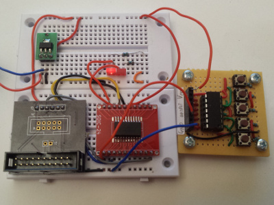
My I2C demo implements a bare-bones write-only master, because getting to this stage of the I2C functionality showing signs of life is by far the highest hurdle. Implementing master reads is just a case of adding in handling of extra states, which the NXP user guide conveniently summarises in a few tables between pages 260 thru 272. At some point I will probably add slave read and write demos, but for the time being I don’t foresee any use-case for having an ARM chips as a slave device. The demo assumed an TCA9535 I/O Expander as a slave device, simply because it was something I had at hand to test with. An existing background with I2C had been assumed as this article is not intended to be a primer on I2C
GCC errors regarding hard floats
For some reason some distributuions of GCC default to hard floats and then complain — as shown below — if the target hardware does not support them. This caught me out as the Windows distributions seems to default to soft floats, which I used for a lot of the development, whereas the SlackBuild ones default to hard. At first I incorrectly assumed this was down to different compiler versions.gpio.c: In function 'ARMirq': gpio.c:31:6: sorry, unimplemented: Thumb-1 hard-float VFP ABI void ARMirq(uint32_t value) ^~~~~~
The solution is to add -mfloat-abi=soft to the makefile, although I suspect it is not the only commandline parameter that can fix the problem.
Unresponsive UART or I2C
A frustrating part of getting the I2C code working is that all the registers mentioned in the relevant user manual section were being set, but no I2C-related interrupts were being generated and theSI flag was never been set. Various Google searches for terms like “NXP LPC11xx I2C SI not set” mostly pointed to NXP’s forum posts that never mentioned any actual solution, and all the sample code I found did not seem to be significantly different to what my own code was doing. In the end the solution was simple: The I/O Configuration Block itself needs to be clocked:
*((volatile uint32_t *)0x40048080) |= 1 << 16
The same issue also affects the UART, but before finding out about the above I assumed problems there were due to electrical issues, so I put RS232 aside and tried to get I2C working instead. It was only a chance sighting of code that explicitly activated the configuration block and the I2C clocks together that I realised what was wrong — aside from the line in Table 21 (page 34) mentioning the configuration block clock, I have so far seen no hint anywhere that a configuration sub-system would be disabled by default.
Remarks
While figuring things out I had come across references to the Cortex Microcontroller Software Interface Standard (aka CMSIS) in chipset documentation, but I never seriously considered using it — it was only after I had written my own mini-abstraction layer that I even looked at CMSIS and found out that it is a cross-vendor open-source project, by which point it was of no value at all to me. In hindsight I most likely would have avoided it anyway, as its multi-chipset nature means I would have to dig through a load of bloat, and many of the bits that would have been of interest to me are written in ARM assembly rather than C — for the time being learning ARM assembly is not an interest of mine. By and large programming ARM is much nearer traditional desktop software development than PIC microcontroller programming, so I classify it separately from the electronics projects I have done over the last 18 or so months.My original motive for getting some ARM chips was to learn more about lower-level ARM programming, because I felt that RaspberryPi was too much of a mini-computer that kept me away from the real grubby bare-metal issues, yet I needed to have experience with getting my fingers dirty with the bare metal of ARM. PIC microcontrollers have served me well, but they are ill-suited for much beyond shifting of bits around in a mostly fixed manner, and are a complete pain for anything approaching structured data. From recent experience I have concluded that the PIC architecture is a pretty unsuitable target for C compilers — in many cases at least a measure of inline assembly is needed, and I am tending towards the opinion that one is better off simply writing entire PIC firmware in assembly. The PIC chips with 1kByte of data memory look like a potential ordeal to use, so this is where ARM comes in.