74HC595 serial-to-parallel chip
22 September 2021The Texas Instruments
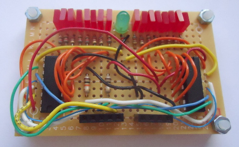
SN74HC595 is a chip that I have experimented with in the past but so far had not used in anything other than that experimental circuit, and the previous article did not include a few critical details.
This article is an update that includes these details, presented here so that I do not need to go trawling through data-sheets to find them, which in turn was spun-out from one of the many projects that got put on the back-burner due to the current pandemic.
Chip overview
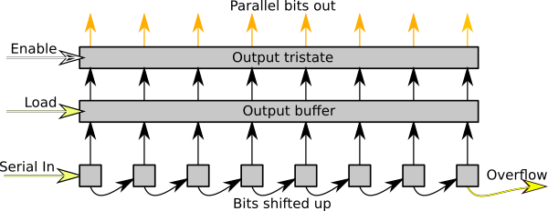
The74HC595 serial-to-parallel chip is summerised in the flow diagram below.
On the rising edge of the clock (not shown) a bit is shifted in from Serial In, shifting the existing bits up one.
On the rising edge of Load, bits are copied from the shift register into the output buffer.
If Enable is asserted the output buffer is output to the parallel output pins, and if it is deasserted the parallel output pins are set to high-impedence.
Note that if the clock and Load pins are tied together the output buffer receives the pre-shift values, so the output is always one clock cycle behind the shift buffer.
Chip pin-out
The pin-out for theSN74HC595N which is the DIP variant of the chip is summerised below; all the other 16-pin variants such as SOIC and TSSOP use the same pin-out.
Unlike a lot of other integrated circuits most of the output pins are contiguous and on the same side of the chip.
I have also come across the CD74HC595 which from a glance over the data-sheet has the same pinning.
| Vcc | Qa | Serial In | Enable | Load Clock | Serial Clock | Serial Clear | Overflow |
| 16 | 15 | 14 | 13 | 12 | 11 | 10 | 9 |
| SN74HC595 | |||||||
| 1 | 2 | 3 | 4 | 5 | 6 | 7 | 8 |
| Qb | Qc | Qd | Qe | Qf | Qg | Qh | Ground |
Note that the pin names given here differ to those given in the data-sheet, and these are detailed in the table below.
| Pin | Description |
| Serial In | New lowest-bit to to shift in |
| Serial Clock | Rising-edge shift trigger |
| Serial Clear | Active-low shift register clear |
| Load Clock | Rising-edge storage trigger |
| Qa-h | Parallel data out |
| Enable | Active-low output enable |
| Overflow | MSB of shift buffer |
| Vcc | Power supply |
| Ground |