Atmel AT28C64B EEPROM
07 May 2021As a bit of a diversion I ordered in an Atmel (part of Microchip)
AT28C64B EEPROM that I intended to use as a programmable logic chip.
As an experiment I wired up the chip on solderless breadboard in order to manually read and write data, and this setup is shown in the picture below.
In the longer-term I plan to make my own computer programmer but before I do that I wanted to figure out how the chip operates.
I would have preferred to use a smaller chip with fewer memory locations but the AT28C64B was the only parallel EEPROM Farnell had in stock at the time.
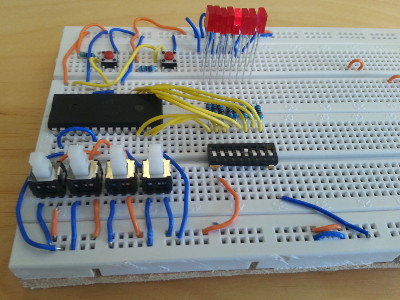
The test circuit
I am not sure where I came across the idea of using an EEPROM as a programmable logic array, but it is done by using the address pins as input and the data pins as output, and exhaustively programming into the chip all combinations of valid input. For the test circuit I used only the bottom four address pins and tied all the others to ground, as for this experiment I saw no real point wiring them all up to push buttons for what is just experimentation. In the future I might rebuild this circut on strip-board with all address pins wired up but I do not have the required resources with me at the moment. For simplicity I tied the chip enable pin to ground and only used the other two enable pins.Although I have no doubt that the push-buttons I am using for the output & write enable will have a lot of bounce, I found that in practice this did not affect how the circuit behaved — I am assuming that any duplicate write operations just happen to all hit the same memory location. The DIP switches I used for writing data have a no-connection middle setting but I found it easier to just pull out the whole switch array before pressing the output enable button — leaving the DIP switches in place while enabling output would short out the data pins.
Chip pin-out and usage
The pin-out for the 28-pin DIP and SOIC packaging of theAT28C64B EEPROM is summarised in the table below; for some reason the pin-out for the TSSOP package is different to that shown here.
| Vcc | Write En. | - | A8 | A9 | A11 | Out En. | A10 | Chip En. | I/O7 | I/O6 | I/O5 | I/O4 | I/O3 | 28 | 27 | 26 | 25 | 24 | 23 | 22 | 21 | 20 | 19 | 18 | 17 | 16 | 15 |
| AT28C64B EEPROM | |||||||||||||
| 1 | 2 | 3 | 4 | 5 | 6 | 7 | 8 | 9 | 10 | 11 | 12 | 13 | 14 |
| - | A12 | A7 | A6 | A5 | A4 | A3 | A2 | A1 | A0 | I/O0 | I/O1 | I/O2 | Ground |
Pins 1 and 26 are unused, and the others are described in the table below. It is unclear to me why the higher address pins are out of order whereas the lower order ones are all in a nice contigious block.
| Pin | Description |
| Ax | Address input |
| I/Ox | Data input/output |
| Write En. | Active-low write enable |
| Out En. | Active-low output enable |
| Chip En. | Active-low chip enable |
| Vcc | Power supply |
| Ground |
Memory reads
Reading from the EEPROM consists of setting the address and then taking the output-enable low, as shown in the trace below; output is maintained until at least output-enable is set high, of which there is no upper limit of how long the output pulse can last. For some reason the dominant factor in how long before valid output appears is the time since the address transition — this is a maximum of 150ns after the transition but only a maximum of 50ns after the falling edge of output-enable. The data sheet does not really commit to any values of how long data output remains after the rising edge.
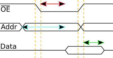
In practice the address can change while output-enable is still asserted although I have not checked whether the data out goes straight from one data byte to another or whether there is a transcient state with the lines being an indeterminate state.
Memory write
To write data to the EEPROM the address bus has to be setup & held around the falling edge of WE whereas the data bus has to be setup & held around the rising edge, both of which is summerised in the trace below. The write pulse width consists of the minimum time between this falling edge and the subsequent rising edge, which is also shown. If more than one byte is to be written which is known as paged mode in the data-sheet, it needs to be started within 150μS of the previous byte otherwise the 10 millisecond write cycle will begin.
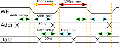
In practice since the specified time for both the address setup and data hold is zero, and the address hold & data setup at 50ns are much smaller than the 100ns for the write pulse width, writing to the EEPROM can be simplified as keeping the address and data lanes unchanged for the duration of the pulse. This is simplification is summerised in the trace below.
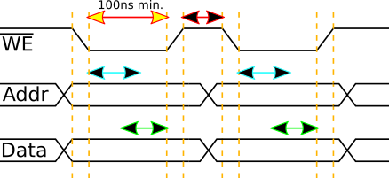
Paged-mode writes
Paged mode is writing upto 64 address locations and then committing them all to memory in one go, because the actual memory programming operation takes many orders of magnitude longer than any other timing factor on the chip. They all have to be on the same page which means keeping the upper address pinsA6 thru A12 have to be kept constant, but otherwise there is no restriction on which order addresses within the page are written to.
Making use of paged mode is just re-asserting the write-enable with new address and data within a quite generous 150μS time limit.
Remarks
I did consider getting hold of some programmable array logic chips to try out, with the Texas InstrumentsTIBPAL20R4-25CNT being one such device I had in mind, but I soon decided that it was not worth the effort of finding a compatible array programmer and associated software.
While the Atmel EEPROM data-sheet gave the reading and writing wave-forms allowing me to design my own chip flasher, the array logic chip data-sheet was basically unhelpful on what programmer I needed to get.
Using an EEPROM as a logic array has some disadvantages such as being relatively expensive, but for my purposes these are not really relevant.