Transistors
24 September 2017Using transistors is one of those things that I was taught in school and have since long forgotten, and the various different ways I saw them explained was as much a hindered as a help. This article is my notes on working out how to use transistors as solid-state switches, and it will cover bipolar transistors as these seems to be the preferred to field-effect transistors for low-current circuits. For my projects I have stocked the following units:
- BC547B - NPN through-hole transistor (Farnell 2453790)
- BC556B - PNP through-hole transistor (Farnell 2453802)
Terminology
Bipolar transistors are current-controlled and have three terminals as shown below. The current Ic that flows through the collector is proportional to the current Ib that flows through the base (middle terminal), and the combined current Ie flows through the emitter (terminal with arrow). The difference between NPN and PNP transistors is the direction of the flow: In NPN current flows from the Collector to the Emitter and is combined with current flowing into the Base; with PNP current flows from the Emitter to the Collector, with some flowing out of the Base.

There are several variants of the bipolar transistor symbols, but the ones shown here are the IEEE 315 ones.
Example switch circuit
Below is a somewhat contrived schematic which shows the simplest way I could think of presenting the use of NPN & PNP transistors as switches. PNP transistors go high side with the emitter attached to Vcc (i.e. current source), and NPN transistors go low side with the emitter attached to ground (i.e. current sink). The collectors of both transistors are connected to either side of the load. The transistors are switched on by pulling the base voltage (middle terminal) away from the emitter voltage, which is done by attaching the bases via a switch to an opposite power rail.
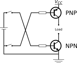
In reality switching on a transistor means having a base-emitter voltage difference of at least (typically) 0.7 volt — and conversely having a voltage drop of less than this to switch it off. In the case of the NPN transistor here the base is powered by a lower voltage level than the Vcc rail, but it will work as long as the voltage is above threshold.
Matching driver to base
A complicating factor is possibly not having control over the type of input that will be driving the transistor's base. For instance the load may have a NPN sinking transistor on the low-side that needs to be driven high to switch on, but it needs to be driven by something like the PCF8574 I/O Expander which is only suitable for driving high-side PNP sourcing transistors. In such a case the driving IC would need to drive a seperate high-side transistor, which in turn drives the low-side NPN transistor connected to the curcuit.
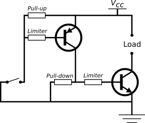
Pull-up and pull-down resisitors have been included for completeness. They tend not to be required for circuits that have actual open-circuit switches, but floating voltages become a headache with circuits that emulate such states using high-impedance output. Normally (at least from what I've seen so far) pull-ups & pull-downs should be around the 10kΩ region, but since in this case the current-limiting resisitors will be of resistances of that magnitudes, my guess is that the pull-up/pull-down values will need to be at least 10 times bigger (i.e. 1MΩ region).
Choosing resistor values
Since NPN & PNP transistors are current-based in circuits that are voltage-orientated, current-limiting resisitors are required. For a demonstration calculation, the following bare-bones circuit will be assumed.
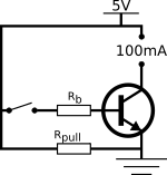
When a transistor is used as a switch, the base current Ib needs to be sufficiently high that the collector current Ic the transistor would be able to pass is higher than the expected maximum current the load requires, which above is 100mA. This is known as saturation and for a given transistor gain of hFE, which can be obtained from the transistor data-sheet, the base current required is as follows:
Ib = Ic / hFE
For the circuit above and assuming hFE is 200, Ib needs to be:
Ib = 100mA / 200 = 0.5mA
The voltage across the resisitor Rb is Vcc minus the transistor's activation voltage of 0.7V, so to obtain Ib of 0.5mA the required resistance is calculated via Ohm's law:
R = V / I = 4.3V / 0.5mA = 8.6kΩ
In reality the target base current of Ib value is a minimum, and since a resistor of exact value may well not be available, the actual base current will invariably be higher. However the amount of excess current needs to be limited in order to avoid problems such as wasted power and overloaded current drivers. For Rpull I would probably use 100kΩ.